This thread has been locked.

If you have a related question, please click the "Ask a related question" button in the top right corner. The newly created question will be automatically linked to this question.

TLC5926 optimal Vout

Other Parts Discussed in Thread: TLC5926

Hello,

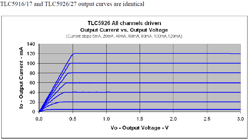
We are hoping to improve our constant current LED drivers using the TLC5926.  Is there an optimal Vout TI recommends for these drivers? The only indication of a Vout range the datasheet provides is the max typ of 17V and ABS max of 20V.  Is there a preferred, or point where it is most efficient to set the output voltage?  My assumption is that this only affects the current regulation of the IC, is that correct? 

Along the same lines, I also assume as long as the IC can dissipate the power, the output pin for the LED driver can reach up to 17V? 

Finally, looking at page 9 of the datasheet, there are multiple examples with corresponding Idd values with the highest one being 25mA.  Would we we add the ~25mA and the total of the current sinked by the output pins  to get the total Idd?  I notice the 120mA*16 is the ABS max of 1920mA, so I wanted to see if I was on the right track.

Thanks,

JC


One person reiterates these output pins can only handle so much Voltage. They are referring to a much lower number of around a volt but i could not find material to back this up. I am just trying to confirm what i am understanding from TI's datasheet on this matter.

  • JC,

    The optimum voltage for the outputs (VLED) is the minimum voltage required to fully turn on the LED at the desired current.  That value is calculated as:

    VLED = VF (maximum LED forward voltage) - VOUT (maximum output voltage for programmed current)

    Any voltage higher than VF + VOUT will be dissipated by the LED Driver.  It will add to the thermal heating of the LED Driver.  The programmed IOUT will not be impacted as long as the required VF is met.

    An LED current of 60mA would require a VOUT of approximately 0.7V.  With a VF of 3V, the VLED should be 3.7V or higher.  Since VF can vary between all channels, the worst case should be used plus desired margin.  For a 4V VLED and an IOUT of 60mA, the driver dissipation for the 16 channels would be (4V - 3V) * 60mA * 16 channels = 0.96W.

    The IDD is based on the REXT being used.  IOUT is based on a current mirror from the REXT pin current (Iref).  Higher IOUT values will require higher Iref values.  The power dissipation due to the IDD current would be calculated as VDD * IDD.  At 60mA for IOUT, the value would be about 5V * 18mA = 0.09W.

    Total power dissipation would be 0.96W + 0.09W = 1.05W.  Using the Power Dissipation Table from page 6, the self heating for a DW package would be about 45.5C/W * 1.05W = 48C.

    The output pins are recommended to operate up to 17V and are tolerant to 20V.  

    Let me know if this helps or you need more clarification.

    Regards,

    Dick

    For the total power dissipation, the calculat

  • JC, the key to a current sink LED driver is to have enough 'overhead' on the current sink pass element to maintain regulation.
    Inside it is a linear regulator, as such it must have overhead to operate in its linear region.
    Below is a graph of Vout vs Iout of the current sink in TLC5926.
    For instance, at 100mA sink you need 0.5V minimum at the IC current sink pin.
    This would relate to the sum of the LED Vf forward voltages in a series LED string, subtracted from the power source at the top LED anode.


    Second question, yes, the voltage appearing at the IC sink output can be up to 17V.
    Operation will be limited by the total power dissipated in the IC.
    Design guidelines would be to assure at least 0.5V at the IC sink pins with worse case maximum LED VF and worse case minimum supply voltage (<=17V).

    Third question, NO.
    The IC sinks current to ground, sourced from the LEDS, so the IC does not provide the LED current, just provides a path to ground.
    IDD current is the current INTO the VDD pin and out of GND.
    OUT0-15 current comes INTO the OUTx pin and out of GND.

    A side note.
    IC power dissipation will be based on 2 things.
    1:  IDD x VDD for the IC quiescent operating power
    2:  Sum of the Isink x Voutx, sum of all the individual OUTx pins sink current and their voltage when sinking (0.5V or greater)

    Does this help?