This thread has been locked.

If you have a related question, please click the "Ask a related question" button in the top right corner. The newly created question will be automatically linked to this question.

-15V output not working in TPS65131RGET

Hi,

I am using TPS65131RGET positive and negative output DC-DC converter in my proto design. In that the negative output was measured at initial power on and noted as -14.9V and positive output as 14.8V.

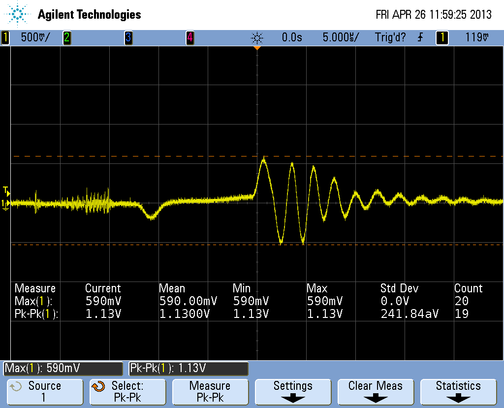
After few days we are again powered on and measured the output as 0.3V at negative output. But the +15V output section was working fine. Then the switching waveforms are probed and noted that switching was not done. The switching frequency waveform taken at power on was attached with this mail.

What are all the causes which stops the switching in IC?.

  • Hello Devendhiran,

    In general it could happen that the layout causes such a problem. Please check out your layout as well as the EVM layout and compare it.

    For a more detailed analysis of the problem, I need the schematic and layout and some more measurements. Please measure the input voltage during startup, the output voltage of the negative converter, the switch pin and the CN pin voltage.

    Best regards,
    Brigitte

  • Hi,

    I have attached layout of  Top layer, second layer, seventh layer and bottom layer (eighth layer) for your reference.

    And also I have probed the output signal waveform, switching waveform, feedback signal voltage and VREF signals at power on.

    The negative  (-15V) was goes to -8V and rose to +12V then damped and settled at  0.3V. The same thing was observed at switching frequency output also.

    The VREF signal was not settled at 1.2V . This also oscillated with 10V(peak to peak) and settled at 0V.

    The feedback voltage was raised to 8V and slowly decays and reaches zero within 40uS.

    I have attached all the waveforms, layout and schematic here for your reference.

    Note : +15V section was working fine and this same circuit was working well in the second module. 

    6886.SCHEMATIC-TPS65131RGET.pdf

    2768.LAYOUTS.zip

  • Hi

    I couldn't the attach the waveforms images with the previous reply, so kindly give me a link/mail ID to send the images.

    Regards,

    Devendhiran K

  • The RC time constant (delay) for enable should be less than 10uS. But, the circuit has a 100 ohms R and a 0.1uF, two 4.7uF 'C' values. The achieved delay is 950uS. 

    This delays the gate control of both Boost-converter & Boost-inverter circuit. Since the Boost-converter gate control has an effect of feedback voltage only, whereas boost-inverter gate control has an effect of Input voltage.(As referred from internal block diagram of IC).

    After removing the additional two no.of 4.7uF capacitors in parallel with 0.1uF in VIN pin, the -15V was settled at correctly.

    Regards,

    Devendhiran K

  • Hello Devendhiran,

    Many thanks for the update.

    Best regards,
    Brigitte