This thread has been locked.

If you have a related question, please click the "Ask a related question" button in the top right corner. The newly created question will be automatically linked to this question.

LM2735 question

Other Parts Discussed in Thread: LM2735, LM3481

Hi all, 

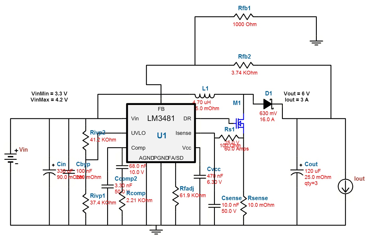
i'm approaching this Ic for an application that require this parameters:

Vin: 3,3 - 4,2V (powered by LiMn battery)

Vout: fixed at 6V

Output current: fixed as high as possibile, 2,5Amps it's good, 3Amps will be great.

Do you think that LM2735 can do my job?

I've also the need to regulate output voltage, i have thought that driving a Mosfet in Pwm obtaining the same current can be a working solution for me, do you think it's realizable?

thanks

Vince

  • Hi Vincenzo,

    The LM2735 does not have enough peak switch current for this load current. We recommend LM3481. Please see attached WeBENCH design. 

    Thanks,

    Anston

  • Many thanks Anston, i have used Webench tool in this day and it's pretty helpful, but i have two problems:

    i would have the possibility to regulate output voltage by trimmer, if i set by pot the output voltage divider without changing tha Caps value, what happens?

    Regulating Vout there is the possibility that Vin >= Vout, so if i've understood i must use a buck/boost, correct?

    thanks lot

    Enzo

  • Hi Enzo,

    You can use a pot/trimmer to set the FB voltage divider. Please note that trimmers are also sensitive to heat. You do not need to change capacitor values when using a trimmer.

    Due to the possibility Vin>=Vout, I would recommend using a buck-boost converter.

    Thanks,

    Anston 

  • hi Anston,

    A customer of mine is evaluating LM3481 but in datasheet it is stated max pk gate current = 1Amp,

    while reading at driver RDSon (and confirmed by test on lab) it is far above (3Amp peak measured)...

    could you confirm me it is a typo error? if not, we have to take care (for reliability) in limiting the pk gate current?

    many tks in advance

    KR

    Vincenzo

  • Hi Vincenzo,

    I need to look into this some more. Give me a day to get back to you.

    Thanks,

    Anston

  • I assume you mean a transient of 3A.  I do not believe that the internal bypass FET can supply that much current for very long.  It may be that the cap on the VCC pin is supplying that transient.  In any case you should not need any external current limiting in a normal application.   If there is a chance that the DR pin can become shorted to ground, then a small resistor in series with the DR and gate of the NMOS will limit the current.

    FD

  • yep, of course, the driving current is not 0 only during the FET transitions, i.e. the peak current (not 0 for the little time the FET needs to switch completely) is around 3Amp, while the datasheet states 1Amp max...

    the question is the 1Amp max is something I have to care about in design or is a phisical limitation of the silicon (i.e. shorting the pin I will never get more that 1Amp)... but this latter seems to be not the case (except of a typo error in the datasheet)...

    KR

    Vincenzo

  • I would follow the data sheet and limit the current to 1A.  If the customer is concerned, they can use a series resistor in the gate lead.

    FD