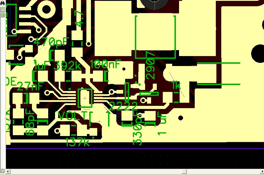
This thread has been locked.

If you have a related question, please click the "Ask a related question" button in the top right corner. The newly created question will be automatically linked to this question.

TPS40210 Current Output Too Low / Early Overcurrent Shutdown

Other Parts Discussed in Thread: TPS40210

Hello,

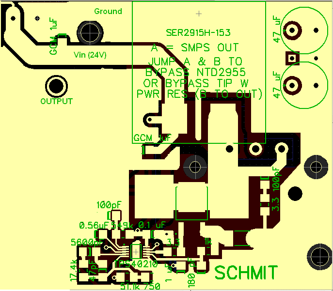
The circuit takes a 24 volt input and bumps it up to a nominal 48 volts. The designed output current using SwitcherPro Desktop is 4.2 amps. The schematic is inserted below as an image. However, when the output is connected to a test load, the switching stops. If the load is gradually ramped down, I can draw at most about 2.1 amps before it goes into overcurrent mode. Typically, it stops switching at about 1.4 amps.

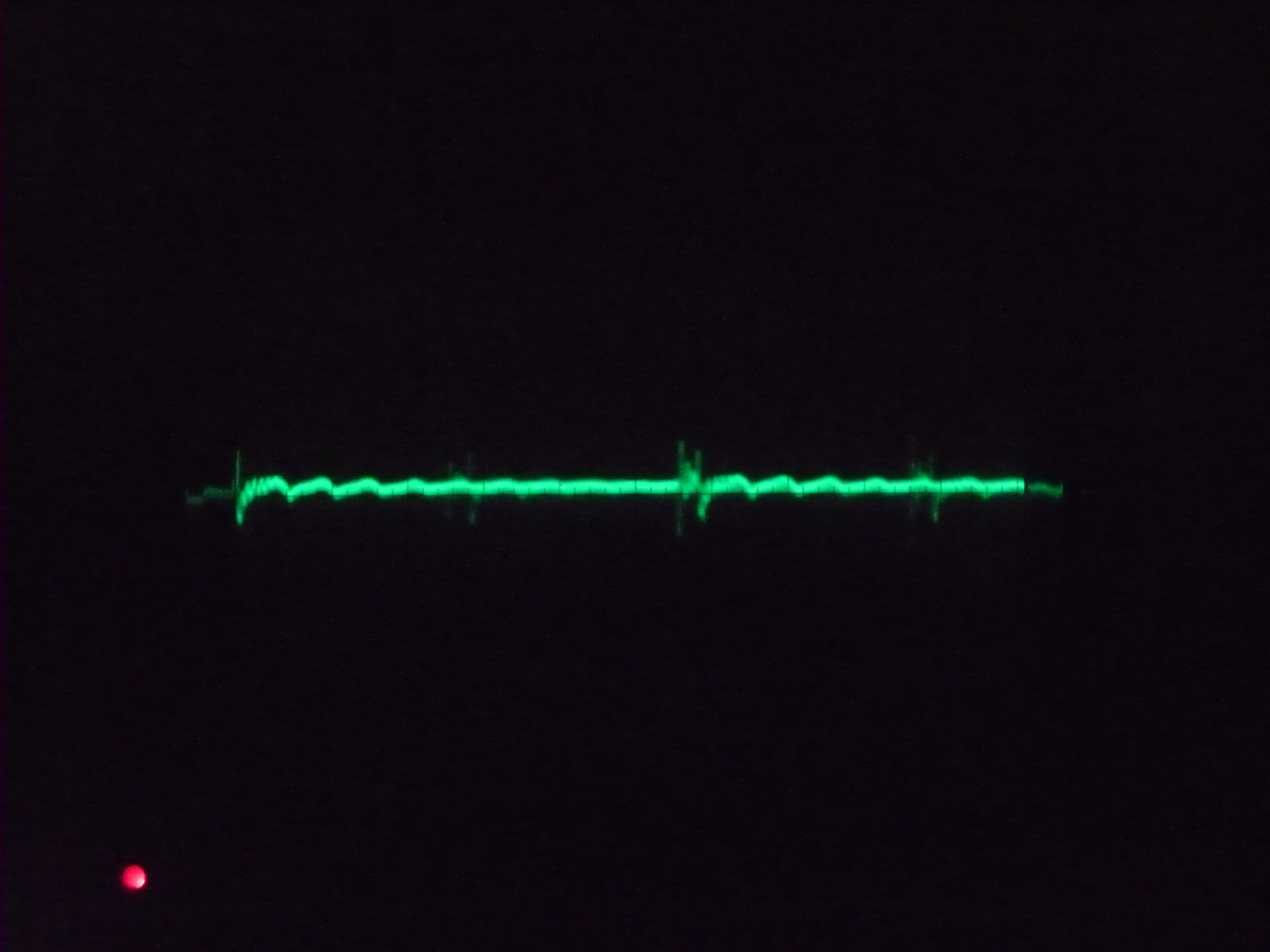
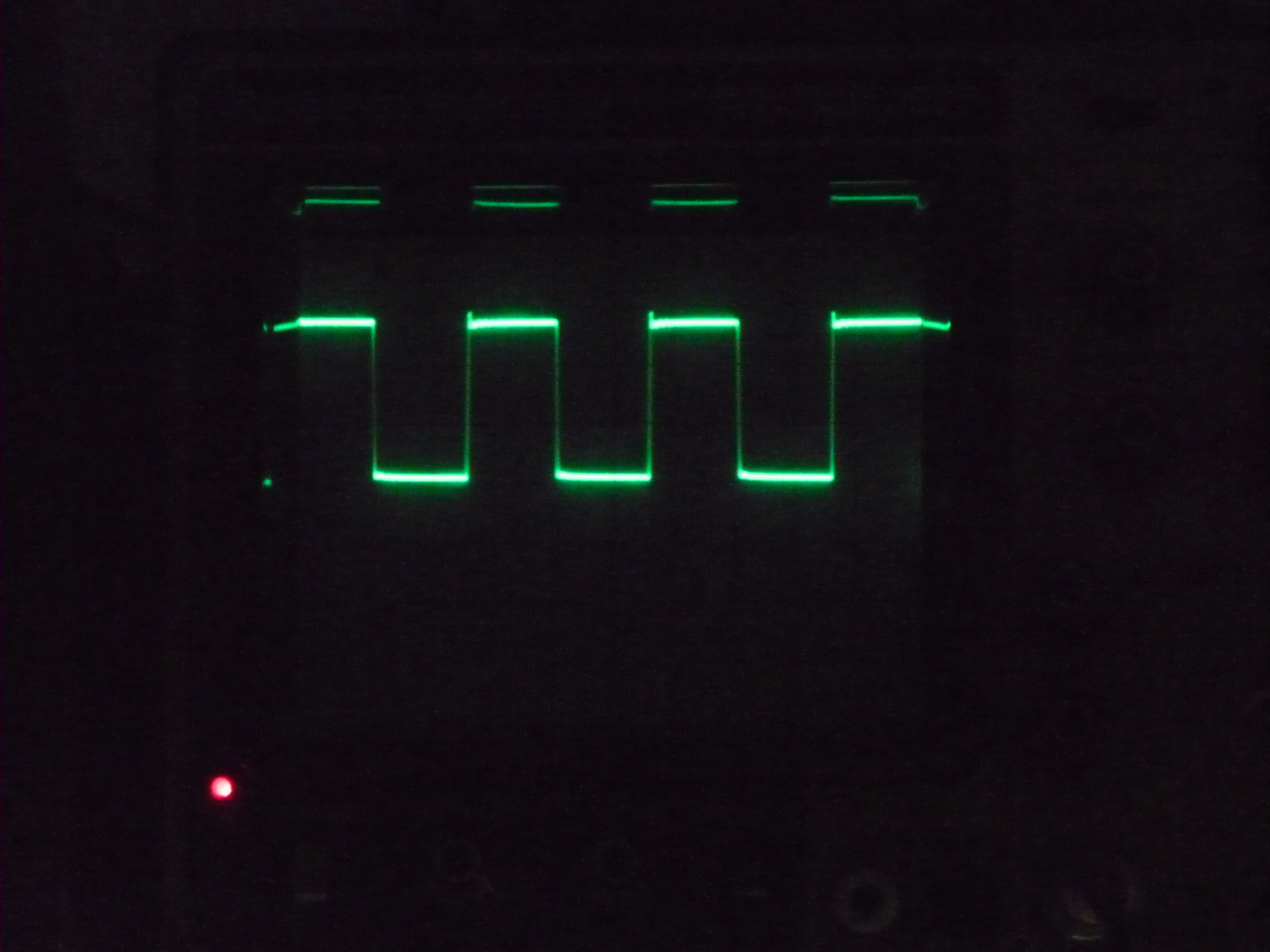
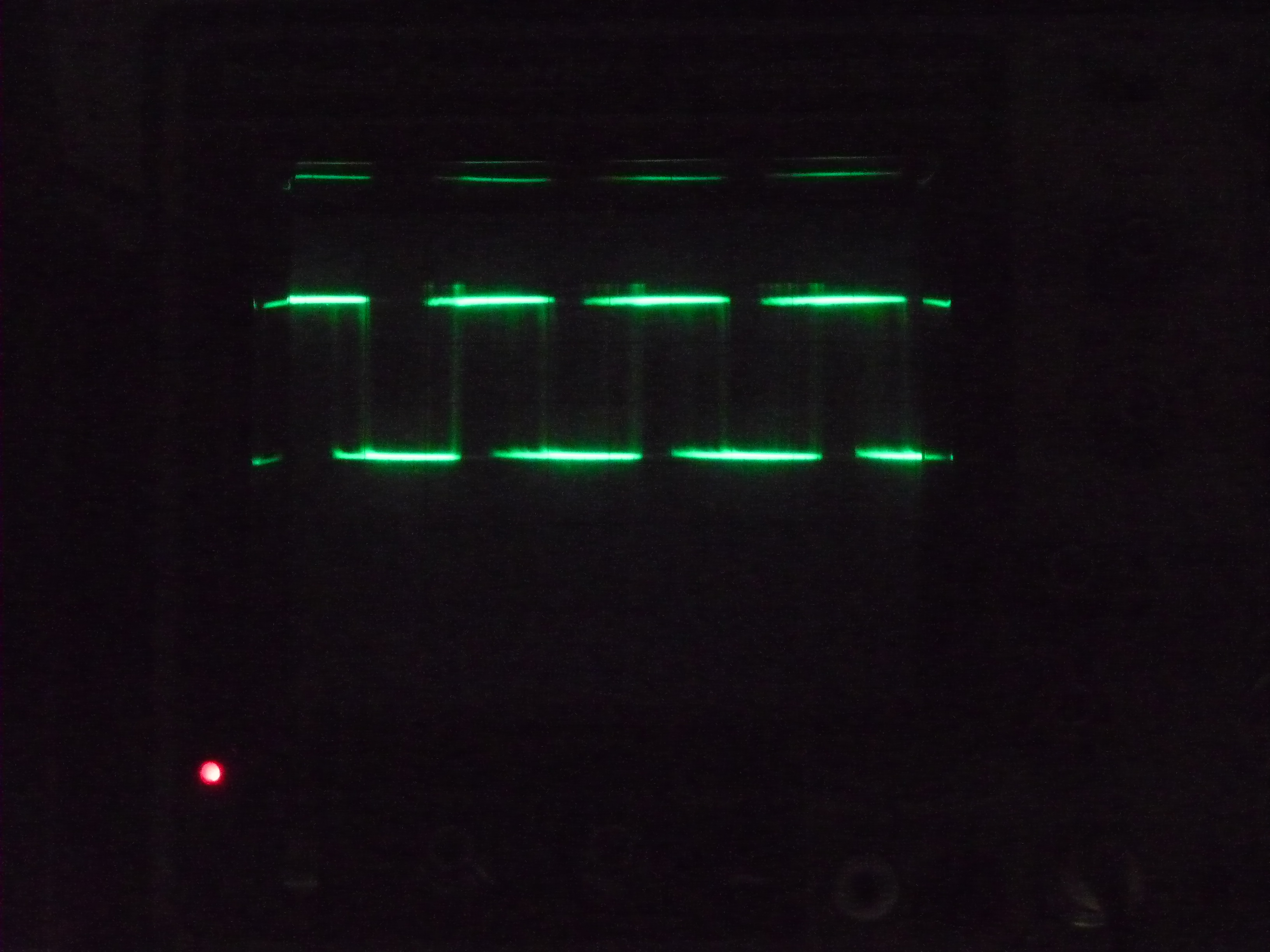
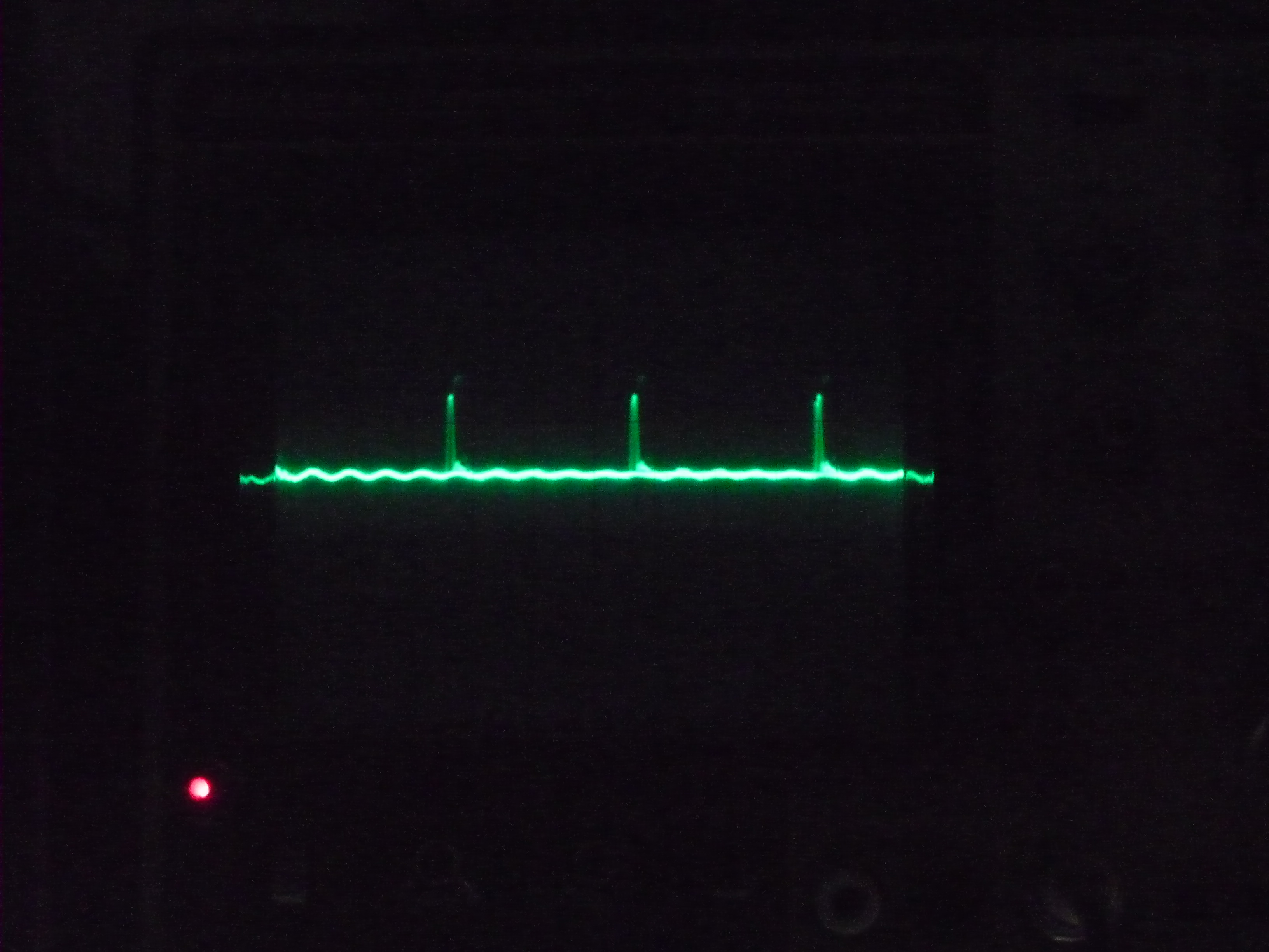
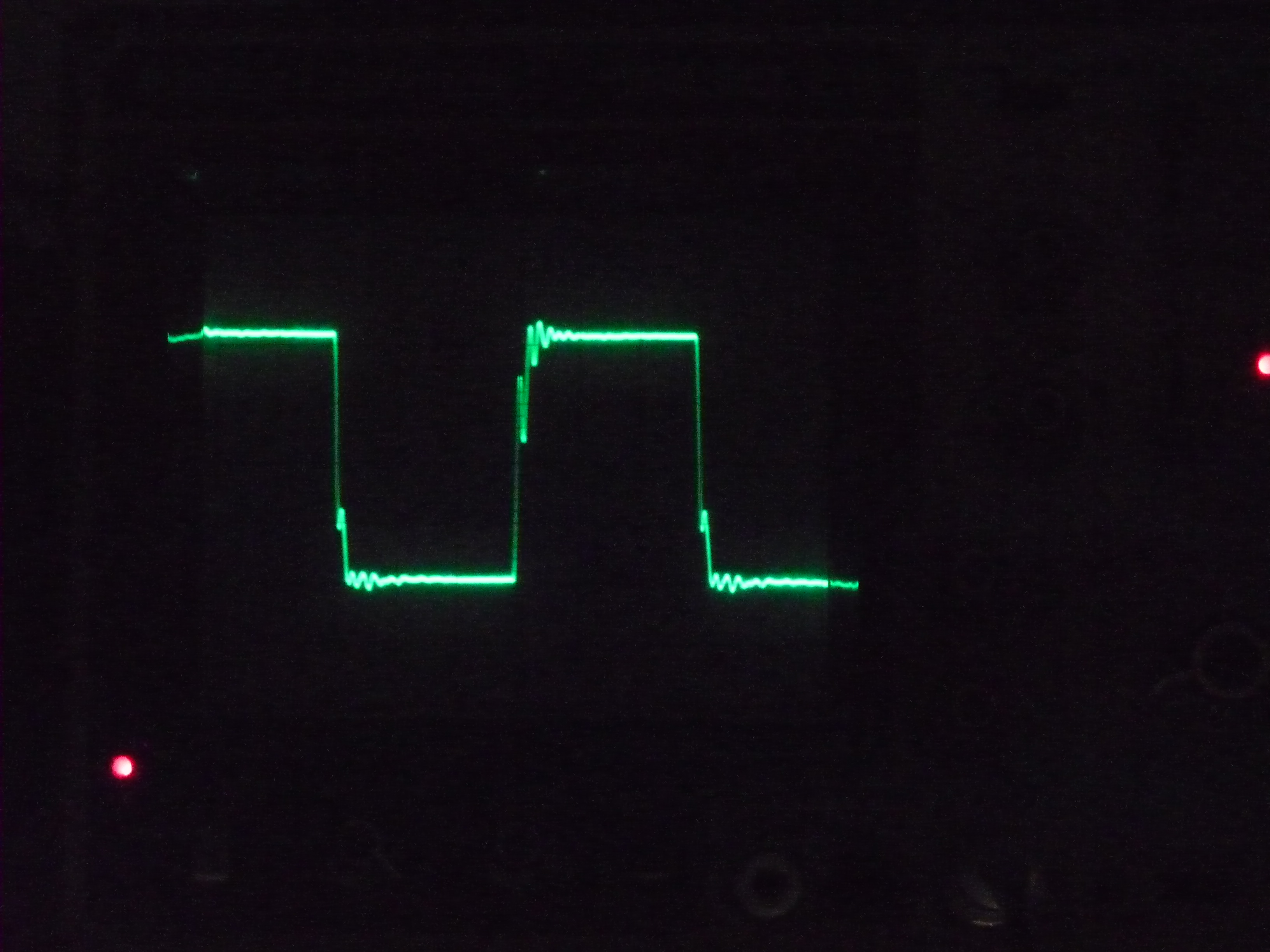
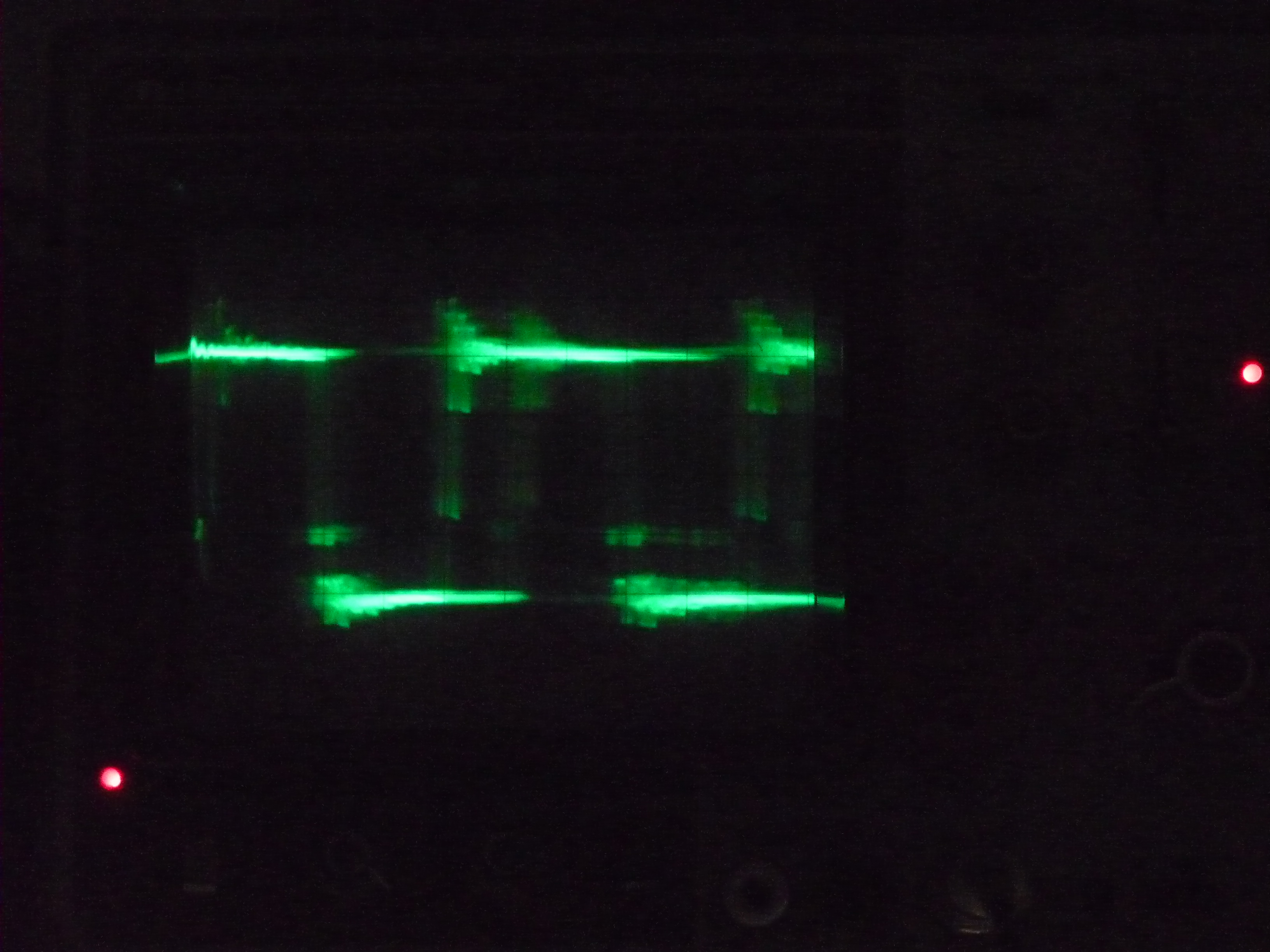
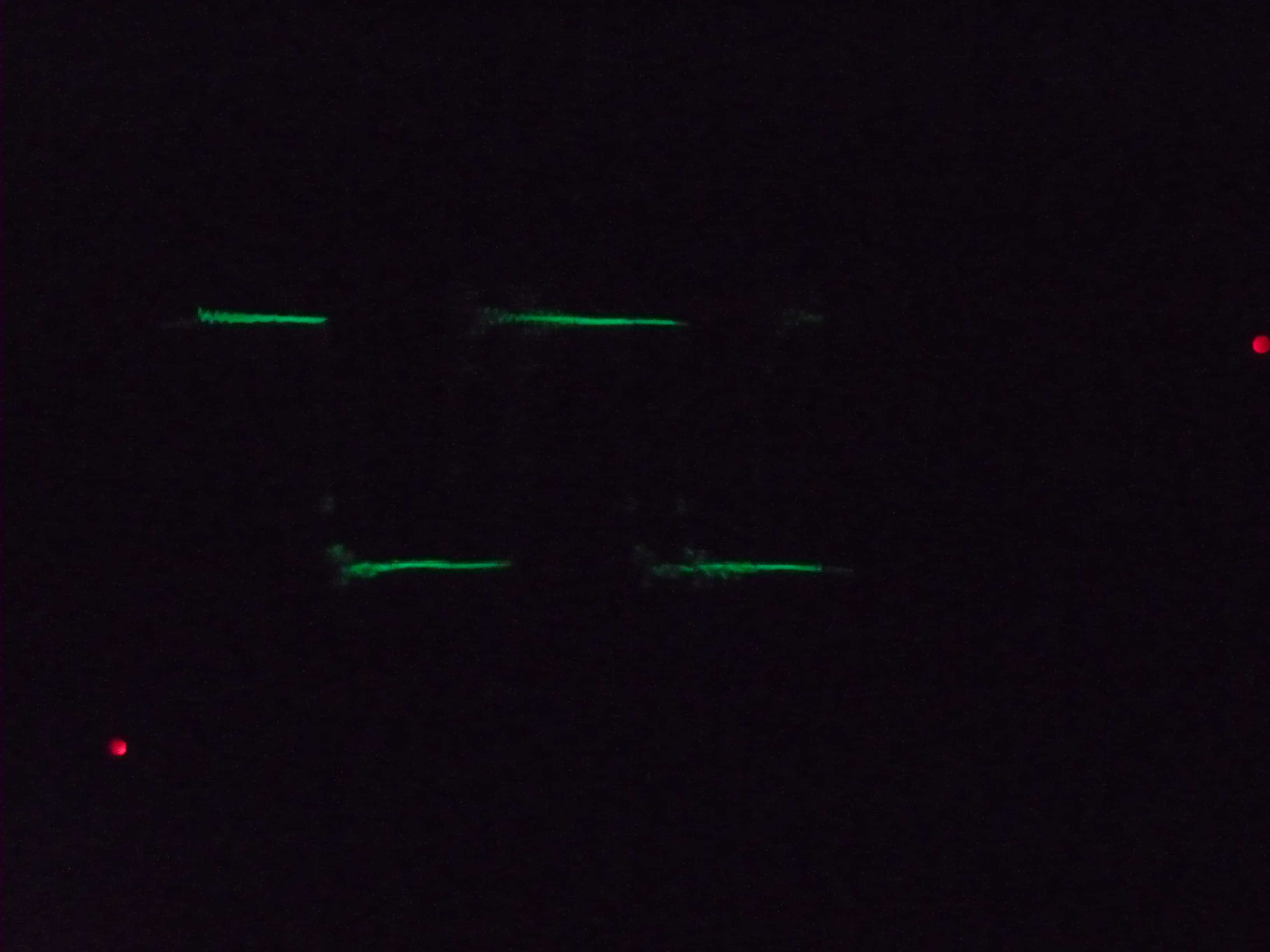
The voltage on the Isens pin reaches a maximum of 40 mV, at which point it stops switching. During the overcurrent situation, the voltage on this pin falls to roughly 1 mV and stays there until retry. I attempted to short this pin to ground in order to see if I could draw more current. While shorted to ground, the controller stopped switching at less than 0.8 amps. 

While there is no load, the FB pin is at 701 mV. As I apply a load, this voltage increases until reaching a maximum of about 737 mV when the controller stops switching.

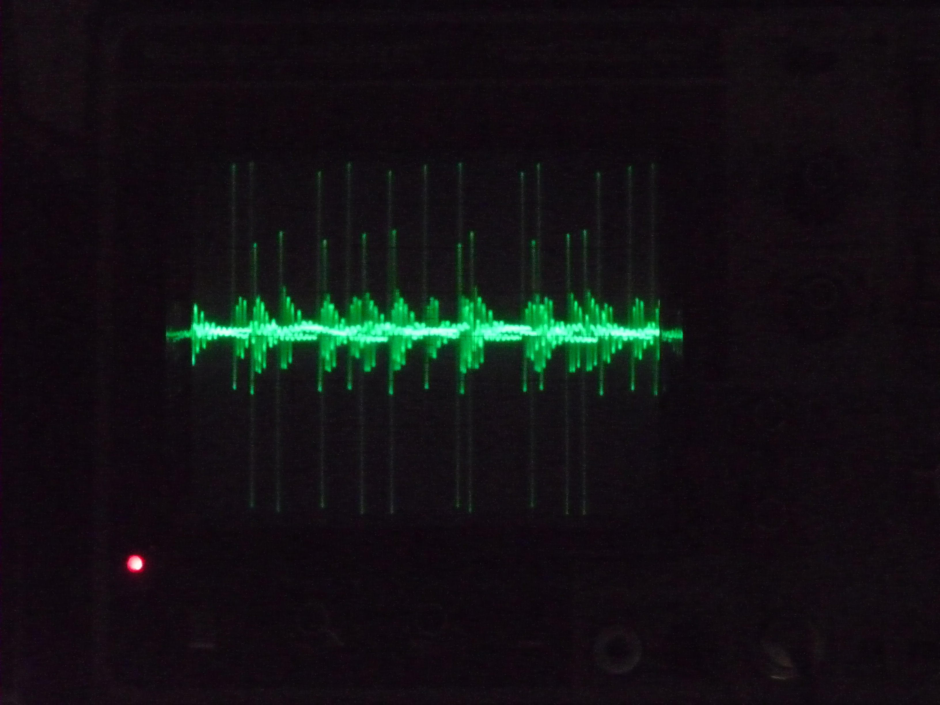
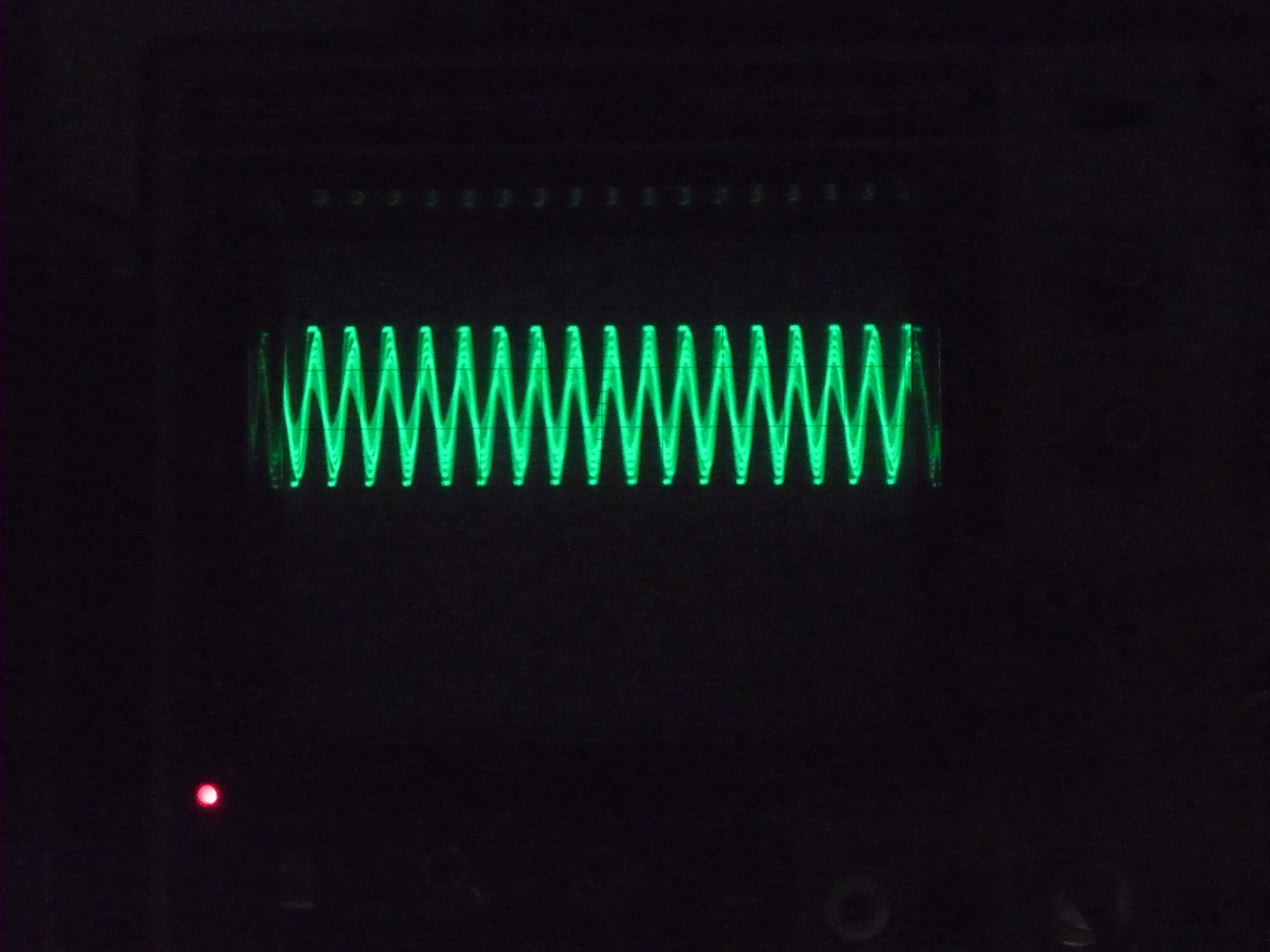
These values were measured with a Keithley 197A DMM. The voltage on the Isens pin as measured by a scope is very noisy. I increased the capacitance from 180 pF to 1000 pF, which reduced some of the noise on the signal but did not improve the situation.  

Any help would be greatly appreciated.

  • Hi Thomas,

    Was this built up on a new PCB? Could you share the layout?

    Thanks,
    Anthony

  • Hi Anthony,

    Yes, this was built on a new PCB. What is the preferred method of sharing the layout? I will post an image of the applicable piece of the board here. The rest of the board consists of low speed analog devices and the testing was performed with these components isolated from the TPS40210 circuit. The switching MOSFET is FDD10AN06A0. This is a 60V 50A N-Channel MOSFET, Rdson = 0.0094 Ohms and a max gate charge of 28nC. (I think the original circuit schematic has a different but similar MOSFET pictured)

    This is only the top layer (2 layer board) and the diode is on the reverse side with a large heat sink. All of the surface mount resistors/capacitors (with the exception of the current sense resistor) are 1206 case size. There is a grounded copper pour around the components. I have removed analog components that were unrelated to this circuit so the pour looks larger than it is in reality. However, this will hopefully give you a sense of how things are laid out. I tried to observe the tips that were in the data sheet regarding placement, but it wasn't always possible.

  • Thanks Thomas, this works. Nothing jumps out at me from the layout.

    A few ideas, can try adding some ceramics in parallel with the 47uF capacitors on the output? What is the part number for the 47uF caps?

    Could you also some screenshots including the switching node, output voltage and gate drive voltage before entering hiccup current protection? Please use a timescale which is small enough to observe individual switching pulses. It might also be useful to catch it right when hiccup is tripped by triggering with VOUT falling.

    Lastly, can you try reducing R11 to maybe 5mΩ? Shorting out this resistor is not a good test because current information it senses is needed for the internal control circuitry in CCM.

    Best Regards,
    Anthony

  • The 47 uF capacitors are rated for 2.6 amps at 100 kHz, 2.9 milliohm ESR, part number: PLV1J470MDL1TD

    I can try adding some ceramic disc capacitors in parallel or, with a little bit of fooling around, I should be able to kludge some surface mount MLCCs to the output. For the revised design, I would be happy to add a pair of ripple current rated MLCCs on the output, if necessary.

    I don't have any current sense resistors below 0.01 ohms, but I will add them to my next Mouser order. I will try to get some screen shots for you this afternoon. Unfortunately, I'm working with an older analog scope with pretty limited bandwidth. Hopefully I can get some decent screen shots using a digital camera on high speed burst.

    Thank you for your help!

  • Glad to help. The ceramics might not do too much with the low ESR of the capacitors you have right now.

    To get below 0.01 ohms, you could also put two in parallel.

  • Hi Anthony,

    I'm sorry I didn't get back to you sooner. This is a pet project and, believe it or not, we had a gas leak in one of our buildings so that through a bit of a monkey wrench into my plans for Friday afternoon!

    I haven't tried changing the current sense resistor yet, but I thought I would share the traces I was able to capture. I apologize for the poor quality. I'm working with an ancient 10 MHz analog scope. I don't have a very effective way of capturing traces.

    OUTPUT:

    No load, 100mV and 1 uS divisions with the scope on AC

    I realize you can barely see the divisions. The blips are separated by about 3 uS and the Vpp is about 100 mV to give you a sense of scale

    50 ohm load, 500mV and 1 uS divisions on AC

    I was running the output to an adjustable power resistor. I put the camera on burst and slid the wiper along until it quit switching. This normally occurs around 18 ohms or so.

    Last image before it stopped switching: 1V and 1 uS divisions on AC

    Switching Node:

    No load, 20V and 1 uS on DC

    50 ohm load, 20V and 1 uS on DC

    Same as before; last image before it quit switching on the same settings as before:

    Gate Drive:

    No load, 5v and 1uS per division on DC

    Now we have gate drive with: 

    50 ohm load, 2V and 0.5uS divisions on AC

    And finally, the same settings as above but the last image before it quit switching:

    (Same thing but with different shutter speed)

  • Hi Tom,

    Were you able to test with the lower current sense resistor? When you test this I recommend increasing C6 to 22nF and reducing R3 to 10kΩ. Reducing the current sense resistor decreases the gain of the control loop so the error amplifier closed loop gain should also be decreased.

    After looking over the screenshots, I see a lot of jitter in the ones taken right before over current is triggered. Does the jitter slowly increase or is it only seen at the maximum load the supply is currently capable of?

    Best Regards,
    Anthony

  • Hi Anthony,

    Forgot to update this thread. I did try the lower resistance current sense resistor. I soldered an axial lead 0.01 ohm resistor in parallel with the surface mount 0.01 ohm resistor. It did make some difference. By slowly "creeping up" on the target current, I was able to get to about 3.2 amps before shutdown. If I simply turn on a resistive load that would draw ~2.5 amps, it shuts down.

    The jitter occurs when I am "creepin up" on the target current. So, with the lower current sense resistor, a small amount of jitter appears around 2.5 amps and gets progressively worse until shut down at about 3.2 amps. These numbers are approximate; sometimes it remains stable until 2.8 amps or so and I get to about 3.5 amps, etc. I will try changing the error amp loop gain in the next day or so.

    I am reviewing a design that you shared in an earlier thread of mine for a 48V 6 amp peak supply. I may end up prototyping that design and see how it works, although I am still disturbed that I don't understand where the flaw is with my current design.

  • Thanks for the update Thomas.

    A couple notable differences between your design and the reference design are the switching frequency and the extra circuit on the gate drive. The reference design uses a slower switching frequency 100kHz. Also the addition of the BJTs Q1 and Q3 help to speed up the turn on and turn off of the FET. Comparing the FET to the one you are using, it has very similar specs in regards to the gate charge. Both of these will help to reduce switching loss and typically have more of an effect on efficiency than false OCP tripping.

    Another thing to try then would be to add Q1 and Q3 to see if there is any improvement.

    Best Regards,
    Anthony

  • Hi Anthony,

    I had a batch of new circuit boards made up following the reference design exactly, with the exception of the switching FET. Again, I used my model instead of the one in the reference design because of it's lower cost and smaller package. As you said, the gate charge and other characteristics are similar. However, I am still experiencing the same problem. At roughly 2 amps, the circuit becomes audibly noisy and the voltage sags. Around 2.3 amps, it goes into over-current mode. I tried further reducing the current sense resistor, increasing output and input capacitance with both low ESR aluminum caps and ceramic caps, etc. Nothing made a huge change in performance. I also decreased R3 from the specified 137k to 51.1k (the next closest value in the same size package I had on hand). It prevents the device from going into an over-current shutdown mode, but the voltage sags all the way down to the 22V in order to maintain roughly 2.2 amps. 

    Also, I have tried a variety of different inductors from 15 uH to 22 uH without any improvement. (I was concerned that my original inductor was saturating but that doesn't seem to be the case).

    Everything works great for lower power situations, but the circuit will be required to occasionally output up to 3.8 amps for short durations. Needless to say, I'm feeling a little disenchanted with my experiences designing DC:DC boost circuits. Any advice?

    Thanks!

  • Hi Thomas,

    Since I don't have any on hand at the moment I'm going to get a board built up with this reference design to help you debug this further.

    Is it possible the 24V input power supply is becoming current limited? I've been assuming not but it's worth checking.

    Anthony

  • Hi Anthony,

    The power supply I've been using is an old HP model with the current limit cranked up to 30 amps and the voltage set at 24.2V. I considered that it may be a problem with the supply so I tested it and noticed the voltage sags about 0.4V from 24.2 to 23.8 volts at 16 amps, which is well within the range of the specified input voltage. I also put a scope on the supply while hooked to the circuit to see how much ripple there was and it was negligible.

    I sure appreciate your time and effort. I hate for you to go through all this trouble; I'm certain the problem is something on my end but I just can't seem to figure out what's going on. 

    A few more details about my design: 

    Aside from the different MOSFET, I am also using a coilcraft inductor. I have tried the following models: 

    • SER2915H-153 (15uH - Preferred)
    • SER2918H-153 (15uH high current)
    • SER2918H-223 (22uH high current)

    I have also replaced R9 and R10 with a single potentiometer with the wiper shorted to one of the pins to use it as a variable resistor. I used this to set the output to 48.2V. Capacitors 1 and 2 have been replaced with a low ESR 2700 uF capacitor with a large ripple current rating. I tried increasing this capacitance to the specified 3000 uF and all the way up to 5400 uF but (as expected) it did not have an effect. The 2.2 uF and 4.7 uF capacitors are "high current" MLCCs and the 470 uF capacitors are low ESR caps. Again, I played around with the output capacitance by adding additional ceramic capacitors and aluminum caps.

    The 48V output is connected to the collector of a TIP142 transistor. The emitter goes through a current sense resistor and then to the load. The current sense resistor is monitored by an AD8211 high-side current shunt amp. The output of the amp is connected to a 2N5551 transistor base which controls the voltage on the TIP142 base by shunting some of the TIP142 base current to ground - thus providing a crude constant current supply. Some time was spent simulating the setup to make sure it was stable and has been used successfully with a constant voltage supply (i.e. 4 SLA batteries!) for some time. This simple circuit is designed to provide 3.6 amps. The main load is only connected for about 0.2 seconds at a time and with a very low duty cycle so there haven't been any issues with the transistor overheating, even when the transistor has to drop a significant voltage. 

    Thanks again,

    Tom

  • It was a bit more difficult for me to get a good board built up with your design than I expected. We actually don't have any designs which used a FET in a DPAK package. I'll need to have something kludged together. Sometimes the packages with long leads can cause some additional issues due to the additional inductance which is why we don't often use them for switching power supplies.

    As a test, is it possible for you to make a FET in a SON package for on your board? Such as the BSC076N06NS3 G recommended from the SwitcherPro design. This could help rule out the lead inductance.

  • Just to be clear, my current board is based around the reference design that was shared in an earlier thread. I am no longer using the design that was originally posted from the SwitcherPro software, although it suffered from the same problem. I have attached the .pdf of the circuit. The MOSFET that was specified in this design was a T0-220 package. With the complimentary BJT transistors driving the gate and with the smaller d-pak design, I find it hard to believe that switching to SON package will improve the situation. (But I will see if I can kludge something together on the test bench - as a small business our PCB manufacturing costs are not negligible, so I would prefer to avoid etching another set of boards until I have something a little more definitive)

    If the lead length really is an issue, I have to believe that the trace length is an issue to, but I don't see how I can get it much more compact with my manufacturing technology. We can go down to 0608 package size for passive components, but we really prefer to stick with 1206 or larger. Similarly, the MSOP package that the TPS40210 comes in is really the limit for what we can handle. The SON packages typically cause us a lot of grief because of our process limitations and the fact that there are no visible leads. On unrelated boards, we've noticed that about 25% of the SON packages end up with solder bridges between the pads, despite the solder mask on the board. We can reduce this number but then we found that we had problems with insufficient solder on larger pads.

    Current Design:

    3716.48V6ASupply_TPS40210.pdf

    Also, here is a screen shot of the board as designed. There are some unrelated components to the left and the inductor, diode and input/output capacitors are not shown. The inductor and diode are directly above the d-pak footprint and all are in close proximity. The "wings" on the d-pak footprint are pads for a board-level heat sink, in case it became necessary. For a sense of scale, the unlabelled IC is obviously the TPS40210 and the passive components are 1206 package. The two BJTs are SOT23 package.

  • Hi Tom,

    I got my board running this afternoon with the DPAK package. I did not see any issues with a 4A load so we need to look closer at what the differences are between what we're testing. I also ran a PSPICE simulation this morning and didn't find any issues. You're right the difference in lead inductance should not make a difference when compared to the TO220 package. I'm really trying to rule everything out since this design should work from what I have looked at so far.

    I'm starting to look very closely at the layout again. Nothing has jumped out me as a clear culprit of your issues yet, although I do see some minor differences in the ground return paths. I've attached the layout of the PMP4540 we have been comparing to for your reference. Please find it below.

    1768.PMP4540RevC Board.pdf

    How do the analog circuitry components compare to the BOM of PMP4540? Such as the components connected to the VDD pin, the ISNS pin, COMP and RC. Are the caps a high enough voltage rating and are they a higher grade dielectric (X5R, X7R, etc)?

    I'm going to try tweaking a few things on my board tomorrow.

    Best Regards,
    Anthony

  • Hi Anthony,

    I glanced over your layout and will study it in more detail this weekend. The majority of the ceramic capacitors are X7R dielectric or NP0 with 10% or better tolerance. I did notice that C15 and C18 are Y5V but I didn't expect that to be an issue with either of these. I believe C15 is just to clean up the internal regulator output and C18 determines the soft start and restart times. Presumably, the higher dissipation factor isn't an issue there. However, next time I place an order, I will add a couple hundred X7R or X5R 1uF caps to the list. We had these ones on hand for another project and figured they would work. Also, the input/output capacitors used are different but with more or less the same specifications. Ours are radial leaded models with slightly higher ripple current rating and are significantly less expensive through our preferred supplier. Also, the voltage rating on the ceramic output capacitors is only 50V - For future designs, I expect to replace these with the following model: UMK316AB7475KL-T (from Taiyo-Yuden)

    Our BOM:4214.PwrSply_BOM.pdf

    Thanks!

    Tom