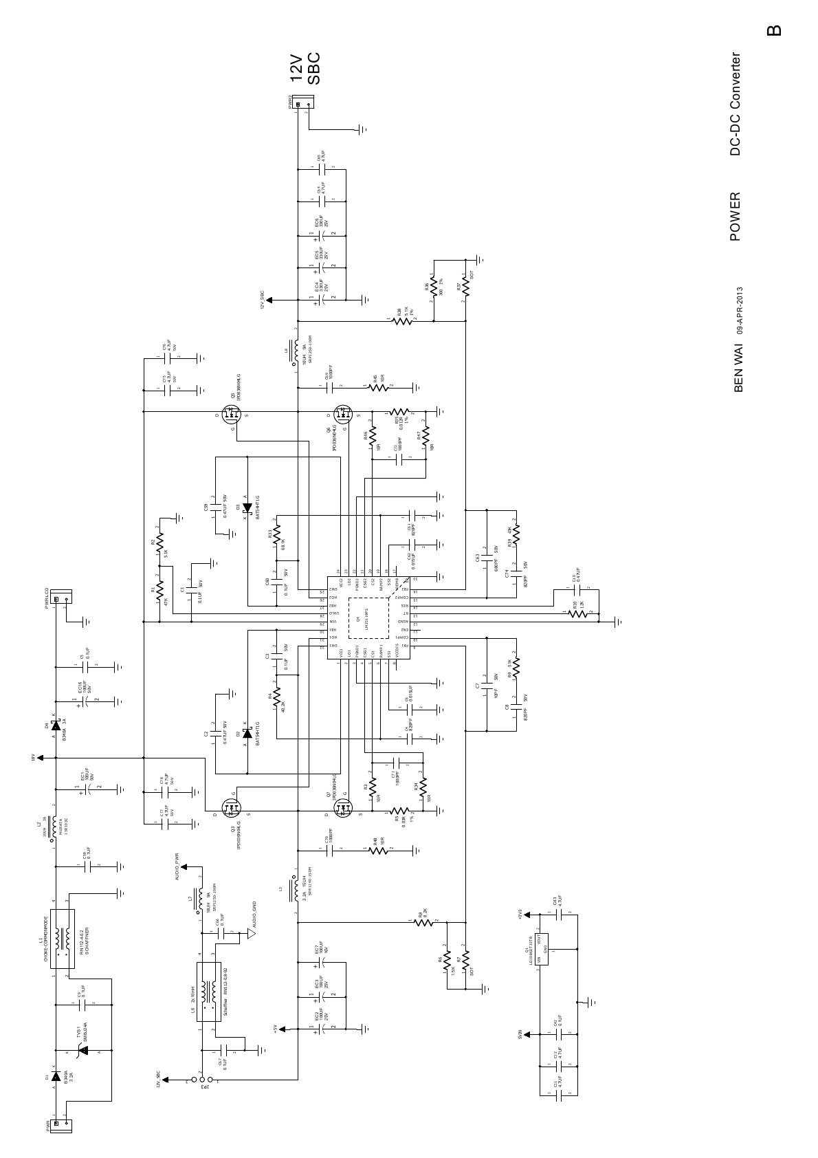
I built a LM25119 with webench assisted values. Input =18V, output 5V and 12V
Outputs are OK but there is heat problem with the controller that it becomes hot(untouchable) in about 10seconds even at no load. I dare not to let it on and load it for more than 30sec fearing component damage.
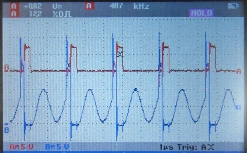
Vcc measurements are different: Vcc1=6.7V Vcc2=7V Not sure if this any hint. waveform capture at HB1 and HB2 is attached.
 HB1
HB1
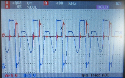
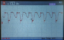 HB2
HB2
Please help and let me know where should I look to.