A related question is a question created from another question. When the related question is created, it will be automatically linked to the original question.
If you have a related question, please click the "Ask a related question" button in the top right corner. The newly created question will be automatically linked to this question.
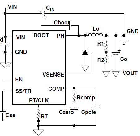
Probably not but it could be. Generally, the thermal pad is the substrate of the silicon which contains a material between it and the exposed pad. This material is not conductive but there may be some resulting Ohms between the die and the pad.
In any case, you must solder the thermal pad to the PCB for the mechanical reliability of the package. While for some devices, you may solder it to a floating connection, the thermal performance of the device is greatly improved when you solder it to a ground plane. For this device. you must connect it to ground per the terminal function table.
We plan on updating the above app note to require a schottky diode on the output, as described in section 4.2 of this inverting app note: http://www.ti.com/lit/an/slva542/slva542.pdf