This thread has been locked.

If you have a related question, please click the "Ask a related question" button in the top right corner. The newly created question will be automatically linked to this question.

TPS53353 Design did not work

Other Parts Discussed in Thread: TPS53353, TPS53355

Hello

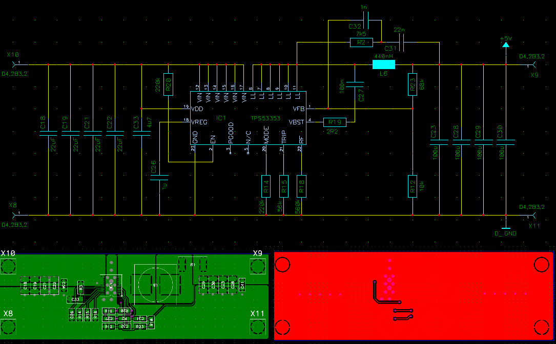
how sensitive the TPS53353 responded to a 2-layer layout?
I make no attempt to run my board.

If I burden the output, the output breaks together

Is a multilayer mandatory?
I think the high MOSFET did not controlled properly.

The Regulated 5V is OK but the PowerGood Pin is low ( with a Pullup Resistor )
Could it be an internal reset that responds to glitches?

  • What is your output current?  I typically find that 2 layers work well up to about 3 A load current.  Is your board shown actual size, or is that just a portion of your board?  I do notice the input capacitors are rather far from the IC.  It is best practice to place them witn a couple mm of the IC VIN pins.  Is there any activity at all on the switching node (LL)?

  • I'm afraid it is not the number of layers that gives the problem, but the locations of the components and ground planes and the length and loops of all traces.
    Try to follow the LAYOUT CONSIDERATIONS gives in the datasheet on page 22.
    For example:
    Place the VIN decoupling capacitors as close to the VIN and PGND pins as possible to minimize the input AC
    current loop.

    Note also that the GND in the datasheet (Figure 39. Layout Recommendation) is 'north' of the IC and far away snubber, boot strap capacitor and ripple injection resistor.
  • Hi Siegfried,

    Please contact Sue Xu (xiao_xu@ti.com) directly. She supports this part now.

    Thanks,

    Nancy

  • The load was only about 200mA.
    On LL Pin was only the output voltage and short spikes on Vin was visible. No Normal On/Off Signals 

    Thanks for the help, I will again make a new test layout.

  • I've seen similar results to what John Tucker described. I have been trying to use TPS53353 for a 5V 14A regulator where VIN=12V. The board is 2-layers. The chip works great for load currents up to 3.85A. But when I tried increasing the load beyond that, the regulator output voltage fails. The chip's internal LDO regulator (VREG) drops below its UVLO threshold. I made sure to get the decoupling capacitors as  close to the TPS53353 as possible but no luck.

    I'm abandoning this part, and I'll re-design the board using something else.

  • I have exactly this problem too (the one described by Kevin Satula).

    Apparently the TPS53353 is simply a defective design.

    Either way, having it perform so badly at the prototyping stage means we will not evaluate it any further and have rejected it as a candidate IC for our design.
  • If VREG is dropping out of regulation, it may indicate that your input supply is falling out of regulation as the load increases. What Are you using for an input supply? The reference EVM works well up to full 20 A load. With a well designed circuit and PCB you should not have any particular issues with TPS53353.
  • (minor correction: I meant to write 53355, not 53353)

    For testing at this stage the 12V supply for VIN is a high-quality laboratory bench supply. VIN has 1u (ceramic), 10u (ceramic), and 100u (tantalum) decaps on the board with the ceramics right next to the TPS53355. I'm quite certain that VIN at the device pins is completely stable and well-regulated.

    And yes, we have an EVM and it does work. But if the chip only works with that exact PCB design and no others, it's a terrible IC. Even if the EVM works properly. The datasheet for this device is extremely poor and I'm sure the EVM designer had access to better TI-internal documentation than the datasheet. If that non-public documentation is required in order to make the chip work then, again, it is a defective design.

    Lastly, I am astonished at the poor quality of error reporting from the device. There are several conditions that could lead to the chip shutting down (UVLO, VIN droop, overcurrent, output-short, etc) and absolutely no indication from the device as to which condition caused the fault. No error register or even a JTAG scan chain. It's basically an un-debuggable device.
  • If you need detailed error reporting, you should probably look at a device using PMBus. Sorry you are having difficulty with TPS53355. Many users are designing successfully with it without any issues.
  • > Many users are designing successfully with it without any issues.

    From what I hear they are mostly at Big Customers of TI who can get the attention of people with access to the undocumented details.

    Just figuring out that the short-circuit protection and overcurrent protection are independent mechanisms (with very different backoff behaviors) wasted a whole day.  No mention of this in the datasheet.  At that point I said to myself "how much more of this chip's behavior do I want to reverse engineer?  Or should I just switch to a chip whose behavior is actually properly documented?"

  • Actually short circuit and over current are the same mechanism as described in section 7.3.6. There is a certain balance between not enough and too much information. However we do assume that the user has a basic familiarity with dc/dc converter operation. Many of the internal details are proprietary and require an NDA to disclose, so we cannot publish them openly. We welcome any suggestion you might make regarding data sheet content.
  • Hello,
    I am facing the same issue. I have design using TPS53353/TPS53355 Vin- 12V , Vout -5V. This design works good for 10A load but as I increase the the load thre is some some sound and also the output becomes a triangular shape waveform. Vin i.e. 12V is stable, on probing VREG i found that there is periodic dip of arounfd 1.3V, and because of this it is failing. I ahve no clus why is it so. Decap is also placed closeby.
  • I think you already have another thread on this, correct?