This thread has been locked.

If you have a related question, please click the "Ask a related question" button in the top right corner. The newly created question will be automatically linked to this question.

LMR62014

Other Parts Discussed in Thread: LMR62014

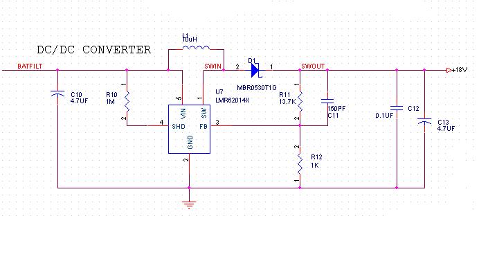
I used Webench to design a DC/DC converter using LMR62014.

Here are the parameters:

vin 9v min, 14.0v max, Vout 18 v @ 0.25 A.

I ordered the parts exactly as specified by the Webench BOM. Built the board, but just cant get it to work. LMR62014 seems to be overheating.

Parts list :

Cin = 4.7uf,

Rp= 4.7K ( Tried 1 M as well)

L1=10uh

D1=MBR0530

Rfbt=13.7k

Rfbb=1k

Cf=150 pf

Cout=4.7uf


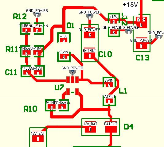
I checked the wiring many times and made sure there were no shorts.

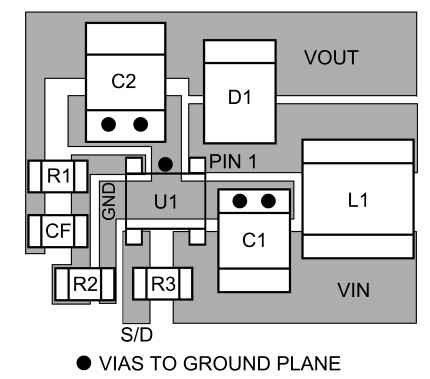
I used heavy traces (20 mils) for all traces and a solid ground plane.  I tried to place the components as close as possible to the respective pins.

I would appreciate any help I can get.

Thanks, Al

  • Hello,

    Can you please provide us with the generated schematic and PCB layout/gerbers.  That way we can review your design and provide you with good suggestions.

    Best Regards,

    -JPF

  • Juan,

    Schematic and Layout for the switcher section are attached. All Ground points are tied to the GND plane on the bottom side. I tried without a load and with different loads. It's doing the same thing.

    Thanks for your help.

  • Hello,

    Thanks for sharing your PCB layout and I think that's where your problem is.  Schematic looks good and component values are okay.  D1 schottky diode of MBR0530 is very good and recommended.  From a layout point of view here are some suggestions for improvement please refer to attached image for a good PCB layout example:

    1) C10 (input capacitor) is far away and GND connection with a single via is not recommended.

    2) C13 (output capacitor) is far away and GND connection with a single via is not recommended.

    3) GND pin connection through single via generates additional noise (high inductance) and current flow is not ideal.

    4) Try to keep GND connections on top layer, with a solid copper plane on the bottom where you can tie GND pin and Cap GNDs through multiple vias (2+)

    5) Connect the top layer traces with ample and generous amounts of copper.

    Your signal integrity, regulation, noise and thermal dissipation will be much better if you follow these suggestions.

    Best Regards,

    -Juan