This thread has been locked.

If you have a related question, please click the "Ask a related question" button in the top right corner. The newly created question will be automatically linked to this question.

LM5116 40V to 24V 10A Circuit. Unstable output

Other Parts Discussed in Thread: LM5116

Hello All,

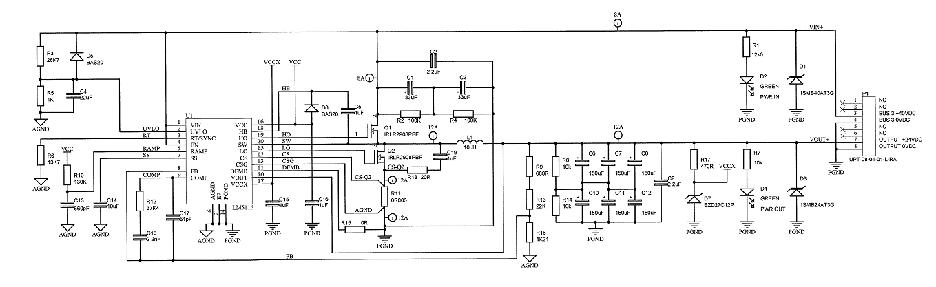
I have prototyped my circuit using the LM5116-EVAL PCB and modified components and the circuit worked fine up to 1A...I have since had some PCBs manufactured andam not seeing a stable output at all. Initially I designed a PCB which had to have a minimum load which wasnt ideal for the application.

The output waveform is sawtooth with a period of around 10ms up to around 4V?

I would like a sanity check on my circuit before I post some waveforms just incase there is anything REALLY obvious I have overlooked, if anyone could take a quick peek that would be much appreciated! :)

Best Regards,

  • Hi

    Here are something you can try.

    - Connect negative connection of R18 to ground.

    - try again after disabling VCCX by connecting VCCX to ground.

    Regards,

  • Hi Eric,

       Many thanks for your reply. I will try the suggestions you mentioned. Just for information I have two variants of this PCB at the moment one which I posted and a second which merely picks up the incoming voltage from different pins on P1...the rest of the circuit is identical. Annoyingly the second variant works fine! Though I havent tested it at full load (10A) yet.

    Looking at the layout for the two PCBs the only difference is that the negative terminal of Rs has the Kelvin connection (shown as the AGND connection to the CSG pin in the schematic) joining directly to the PGND plane in the second PCB. In the first PCB (which is not working) the kelvin connection is as intended.

    I have already joined the CSG pin directly to AGND at the chip and this made no difference in the operation of the first PCB. I feel this might be mere coincidence as it seems not enough of a difference to make it unstable?

    At this point I have ordered some replacement LM5116 chips as my gut feeling is the chip has been damaged during assembly or handling. We observe ESD precautions here but I cannot confirm that it has been fully adhered to!

    Whilst I am waiting on the replacement chips I will try your suggestions.

    Best Regards,

  • Hello Again Eric (and everyone).

    I have replaced the LM5116 and still get the same behaviour.

    I scoped the VCC terminal and noticed a dropout at the peak of the sawtooth waveform. I also noticed this on the PCB which is working.

    My guess is that this dropout occurs when the internal regulator drops out in favour of VCCX.

    Next I removed VCCX from operation by removing R17 and D7 and shorting VCCX to ground (as suggested).

    The PCB now starts up and I get a stable 24VDC even at no load which is excellent!

    My theory is that the current available to the IC (via R17) is not sufficient enough at the lowest point of VCCX (4.5V??) during startup. I have ordered some smaller resistors to put in place of R17 to get a better current availability on startup (390 Ohm and 330 Ohm).

    I would like to get some more opinions on this...what do you guys/gals think?

    Best Regards,

  • Hi Again all,

    I have been testing the modified circuit now (as discussed previously). I have successfully got the load up to around 3A (using halogen bulbs as the load).

    I have run into a problem, on switching a slightly larger load (~3.5A) on the PCB appeared to run into current limit (the output LED was flashing).

    The circuit will now not function correctly, at open load I get around 3V average??

    Taking a peek at the output resistance I see a steady 4Ohm (approximate) resistance which is not good! In the circuit I have replaced the MOSFETs with some that have a lower total charge (to ensure I dont hit the current limit of the internal reg) and roughly 1/10th switching time (tr and tf) to reduce the power dissipation.

    Could these better(?) MOSFETs have caused the issue??

    I havent yet replaced anything on the PCB to see if the IC(for example) is damaged or not yet.

    I suspect the snubber components I have on the PCB might not be sized correctly for the increased switching speed of the newer FETs? Is there a rule-of-thumb for the snubber components or do I literally need to scope the switching node and calculate based on that??