This thread has been locked.

If you have a related question, please click the "Ask a related question" button in the top right corner. The newly created question will be automatically linked to this question.

TPS5410: Oscillaton on the ph pin

 Hello 

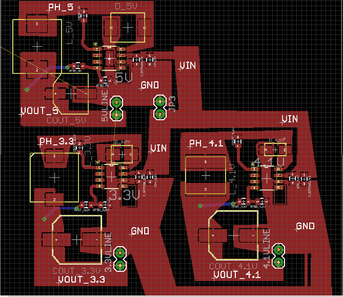
I have a similar issue with my TPS5410. The attached waveform show what I get on the PH pin on 2 of my chips for different output voltages. As you can there is an oscillation in there. I have used the online tool and schematic and the recommended layout on my board also. I also have attached my board layout.

Thanks

ph53uin_.tif
  • Hi Gary,

    Thank you for your interest in TI parts.

    The waveform you posted shows normal operation for a non-synchronous Buck (catch device is a diode) when the inductor current is discontinuous. I don't know what your design parameters are, but assuming you have appropriate component values, the inductor current will fall to zero when the load current drops to less than half the inductor pk-pk current.

    So for example, if the inductor pk-pk current at a given operating point is 0.6 Apk-pk, then the inductor current will fall to zero when the load current drops below 0.3 A dc. When the inductor current falls to zero, then the PH node or PH pin is free to move anywhere between 0V (clamped by the catch diode) and +Vin (clamped by the body diode of the HS FET). The PH pin will eventually settle out at Vout if given enough time, but since it usually starts at 0V, then the parasitic capacitance at the PH node will ring with the output inductor. That is the sinusoid in your waveforms.

    A rule of thumb for the inductor value is such that it results in a pk-pk current of about 20% to 30% of the full load DC current. So for 1A full load DC, the inductor should be sized so that the inductor current is about 200mA pk-pk at your nominal input voltage. This would mean that the PH node will start to ring as shown when the load drops below 100mA DC.

    Regards,

    MC.

  • Hi 

    These are the parts I am using for my design

    Thanks

    webench_design_3528983_70_609255942.pdf
  • Hi Gary,

    OK, with 500kHz, 33uH, Vin of 8.5V and Vout of 4.1V, then the inductor pk-pk current will be approximately 129mA pk-pk when continuous. The inductor current will fall to zero within each cycle during the (1-D) when the load current drops below 129/2 = 64.5mA DC. So at loads below 64.5mA DC, you should expect to see ring-out as shown in your waveforms. The threshold of continuous inductor current will be dependant on operating point, including Vin. So if Vin changes (or Vout, or Fsw, or L), the threshold of discontinuity will change.

    When the load is greater than this 64.5mA, then the PH node should be a typical PWM square wave, with a high of Vin, a low of 1 diode drop below ground, a duty cycle of approximately 4.1/8.5, and an ON time of (4.1/8.5)*(1/500kHz).

    As the load current drops slowly below the continuous threshold, the PH waveform will transition from the PWM square wave, then there will be some lifting above ground just before the ON pulse. As the load drops further, the lifting will transition smoothly towards a sinusoid ring-out.

    Regards,

    MC.

  • I have attached what ph looks like at 700mA .I need to remove that ripple as best I can as it is coming back on my output at about 500mV pk-pk? How can I remove this, a rc snubber has been suggested but I am unsure how to design one, as I created one but it made it worse? I would like to the the noise down as low as I can?

    Thanks

    ph700ma.tif
  • Enclosed is a document on RC snubbers:

    5545.RC Snubber.doc

  • Is the oscillation period where the ripple peaks to where it settles down because the diagram isn't the most clear?

  • Hi Gary,

    I'm sorry, I misunderstood to which oscillation you were referring. The oscillation at the front end of the high pulse is not related to the above discussion.

    The ringing in your latest snapshot is due to the recovery of the catch diode along with parasitic elements in the layout. The ringing can also be the result of non-ideal layout even without diode recovery. The amplitude you posted really isn't that bad or uncommon and will be difficult to reduce without a hit in efficiency. The best way to minimize this ringing is with good great layout, but you already have your layout done. So the next thing you should try is indeed an RC snubber. Given your schematic and operating point, I would start with a C value of 680pF and an R value of somewhere between 50 and 60 ohms. The RC should be placed right across the PH pin to the ground pin, which is the same as saying right across the catch diode. The suggested values will incur a hit in efficiency of about 1%, or about 25mW. If the snubber is placed too far from the PH pin it will not help with the ringing (but it will still eat up 1%).

    I suggest putting the R to the ground side and the C to the PH node. Functionally it makes no difference, it's just easier to measure the resulting rms voltage in the R if it isn't flying.

    When you measure the output ripple, it is important to follow good high frequency measurement methods. This implies an extremely small probe tip and equally short ground lead on the probe, see attached picture. Measure right across a ceramic output cap. The typical scope probe leads are far too long and will yield high frequency spikes and ringing that are not necessarily realistic. Don’t use the long ground lead included with the scope probe. Usually there are smaller clips included in the package, or you can make one yourself. For noise measurements like this, measurement technique is crucial.

    Where and how are you measuring the ripple?

    If you have the chance to improve the layout, there are suggestions I can offer.

    Regards,

    MC.

  • I could give you my files that I used in eagle to design the board?

  • Hi Gary,

    Let's take this offline. Please provide an email address I can use to contact you.

    Regards,

    MC.

  • Yeah I was going to suggest that before giving files. Its gnorris@scorpionnetwork.com

  • Hi Gary,

    I tried emailing you directly to the address provided but it bounced. Please check the address and if it is correct then we'll need some other means to proceed.

    Regards,

    MC.

  • Hi sorry left out an s. Its gnorris@scorpionnetworks.com

  • I'm confused about the design example and it says the oscillation period is 24.8ns but in the plot the divisions is 250ns. So I guess my question is the oscillation period the time from where it peaks to where it settles?

  • That dsign example does not really go into the detail of measuring the ripple.  I think the author assumes that you will know that.  He probabl zoomed in on the waveform to measure itt, but did not include the zoomed in wavform in the document, only the "before" and "after" waveforms.  The "period" he refers to is T = 1/f, whwre f is the frequency of the ringing.