This thread has been locked.

If you have a related question, please click the "Ask a related question" button in the top right corner. The newly created question will be automatically linked to this question.

LMR62421 keeps burning out

Other Parts Discussed in Thread: LMR62421, TLC59108

I'm using the LMR62421 to boost a 3-5V input up to 15V to run a string of LEDs.  While it's a great solution when it works, I've been having them burn out on me on a frequent basis, and I can't figure out why.  The standard failure mode is that while all of the inputs are where I expect, the chip simply stops switching (as confirmed by scope on the SW pin).

I'd been thinking that somehow the changing weather had caused me to damage the chips via ESD, but after the most recent one I don't think that's the case: I had the completed board sitting on a wooden surface with a 5V power supply.  I checked for about an hour that it was working properly over an output current range of about 5-120mA, then left the board powered on a very low standby draw for several hours, after which it was still working fine.  I then left it overnight and checked the next morning, at which point the chip was dead.  The control IC on the board still talks, and the high-side output is still connected at about Vin, just as if the chip were in shutdown mode, but EN is pulled high by a hard-wired resistor.  I don't think that temperature could have been an issue, and the load on the system was trivial.

I've seen this failure mode a few times now, and I've been able to repair the boards by replacing the IC, but I can't figure out what keeps causing them to burn out.  I'd appreciate any troubleshooting pointers.

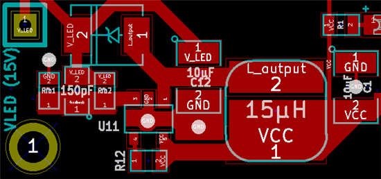
The layout is mostly cribbed from the demo board, and the external component selection was taken from WEBENCH, with the exception of a beefier input capacitor, which also serves as transient protection in conjunction with an upstream protection chip.  The schematic is verbatim copy-and-paste from WEBENCH (equivalent to boost design examples 1-3).

  • Hi,

    Our team will review your PCB layout and application.  How many LEDs are you running and what's the part number for these?  Was this application running before for prolonged periods of time and just recently started failing?

    Best Regards,

    -Juan 

  • I'm running 6 strings of LEDs with total Vfs of around 13-14V from the V_LED rail, which is boosted to 15V.  They're feeding into a TLC59108 that's set at a constant current of about 20mA per string.  Tests with an Agilent bench supply indicated a maximum input draw of just under 0.7A at 3V with all strings at full brightness.

    When the latest LMR62421 failed, it had had a total runtime of 10-15 hours at output draws ranging from 5-120mA.  It had been sitting at idle, with most of the strings fully off and one at a token brightness, when it stopped switching.  This is a new design, and I've had the issue with the LMR62421 repeatedly with it.  It's entirely possible that I put some stupid bug into the board, but I don't see where it could be given that the switcher does work completely correctly until it doesn't (I can spin the input voltage up and down and the output rail never has any issues), and the output circuit is literally just 6 series strings of LEDs absorbing most of the voltage until run into a correctly-working constant-current drain.  (I'm happy to attach source files if they would be helpful, but I'm not sure what you'd need.)

  • Update: I just repaired one of my boards with a new LMR62421and watched it stop working. The board had been running for about 3 minutes and was in a steady-state input current of about 190mA at 4.7V from a bench supply (about 60mA output at 15V) and then simply went dark.  I'm seeing the same failure mode (the switch pin appears to have simply stopped switching). Nothing was under any interesting load, and no connections moved or were switched.

  • Hello Chrilis,

    From the information you have provided so far, the only thing that does not look right is the component placement for your Diode and Output capacitor.  When I follow the current and voltage path to the output:

    1) You're taking the output voltage to the LEDs and also the FB voltage (from the resistor dividers) directly from the output of the SW diode.

    2) The output capacitor is connected and placed relatively far away, therefore minimizing any effect on the spikes/output ripple at the cathode of the diode.

    3) Your ground plane on the top layer is severly minimized due to your component placement and it's relying on a single VIA on the output cap and below the SOT package to carry all the current to the Ground Plane

    4) The ground connection of your 10uF input capacitor goes through a very thin trace and through a single via to the ground plane.  Even though, input capacitor is not that important on a boost regulator, the relative position and GND connection make your input capacitor almost non-existent for this application.

    5) Please show your ground plane PCB

    Please connect a scope and capture the voltage right across your LED's, Test Point V_LED:

    1) Make sure you use a short ground connection for the probe to minimize ground ringing to be introduced into your measurements.

    2) Also show the pin #1 (SW pin) on the scope

    3) Since your failure rate is very consistent, please capture the above 2 waveforms before and during failure mechanism.

    4) You can try and ADD another 10uF output capacitor next to the Diode and place it's ground connection on the top plane if there's a top-layer GND plane available close by.

    Best Regards,

    -Juan

  • Thanks for the specifics; I've been mostly a programmer up to this point and am not yet familiar with allof the layout rules that are necessary for high-frequency circuits.

    1) This doesn't seem to be causing noticeable issues when the circuit is running, since the LEDs are insensitive to ripple and have further bypass capacitors next to the V_LED taps, but I do see the difference between my setup and the one on the demo board.  Should the feedback tap be between the diode output and the output capacitor?

    2) I'll try to rework to move it closer.

    3) I'll see what I can do about the ground vias, but I'm limited in how small I can make them by my prototype fab (in particular, no microvias), and I was trying to keep the components as close together as possible, which limited the number of vias I could insert.

    4) I'll keep the distance in mind; I didn't realize that that short of a separation attenuated the capacitor's effect so much.  (The capacitor is actually placed so it's adjacent to a power-protection IC that's just off the diagram, which I cropped because of forum width limitations.)  I definitely should have made the trace much wider.

    5) The ground plane (on my 2-layer board) is flooded across the entire backside of this area.

    Since I've used up my run of prototype PCBs, is there any problem with moving the (revised) layout onto its own breakout PCB for testing purposes and then copying-and-pasting back onto a larger board as long as I have connections that can handle the appropriate currents?

    I'd be happy to try with a scope, but while I've had consistent failures, the timing has not been predictable, and I am not sure that the scopes I have access to can capture a continuous stream.  I'll check.

    Thanks for all the help so far!