This thread has been locked.

If you have a related question, please click the "Ask a related question" button in the top right corner. The newly created question will be automatically linked to this question.

Synchronizing the TPS40210

Other Parts Discussed in Thread: TPS40210, TPS40200

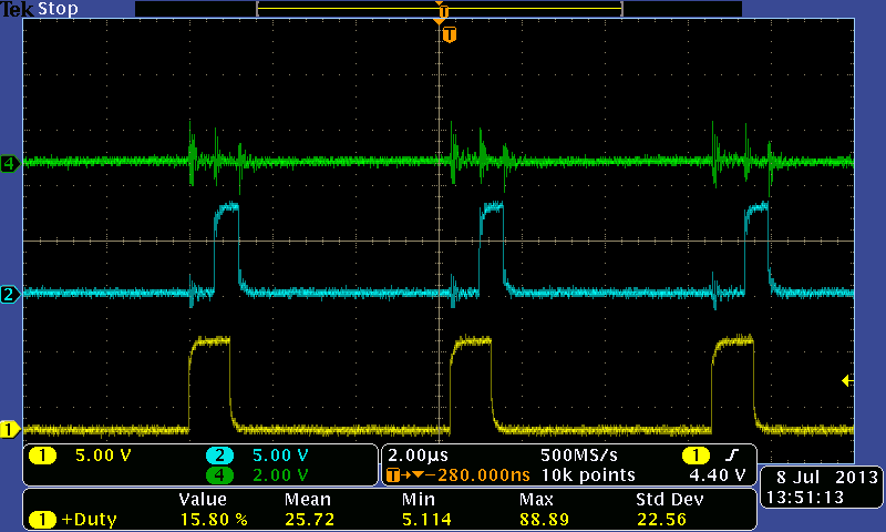
I set the RC to 500K and 470pF which has the Controller running at ~ 100KHz, then using a 1N4148 Diode with the anode connected to the RC junction per the Data Sheet

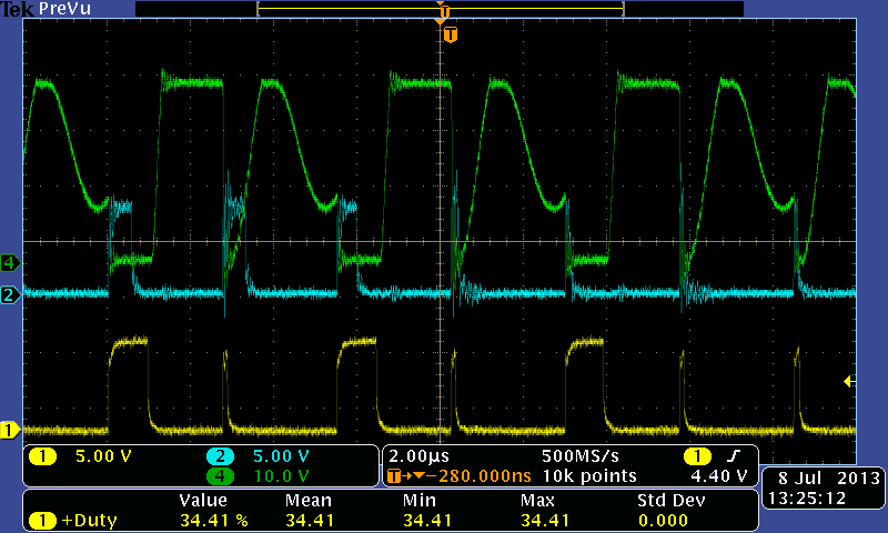
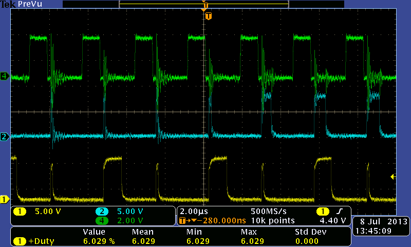
I applied a 5V, 250KHz clock with a 30% Duty Cycle (positive) through a 5.1K resistor. The controller does not seem to like this as I get occasional double pulses and the controller restarts every 100 ms or so. The controller works fine when I disconnect the external clock and set the RC time constant for 250KHz and the Duty Cycle at full load and minimum Vin is ~ 43%............the Data Sheet offers little info on synchronizing the TPS40210 so am I missing something here?

  • I made a mistake in my first post, the diode is connected to the RC junction by its' CATHODE per the Data Sheet....

  • Hi John,

    I did not notice anything incorrect with your description on how you tested this. For some clues, can you share a screenshot of the waveform at the RC pin, the input clock signal and the VDS voltage of the FET?

    Best Regards,
    Anthony

  • Anthony,

           According to the Data sheet, the Cap charges up to approximately Vin/20 through the external resistor then the cap is discharged through an internal Transistor of the TPS40210. The data sheet shows the RC junction goes to an internal Window Comparator where it is compared to a 150mV reference on the low side and a Voltage divider that is referenced to Vin as well. The comparator outputs go to the Set and Reset lines of a S_R Latch and the Q output of the latch is used to control the discharge transistor. If the transistor is turned on instantly when the RC pin rises to Vin/20 which the block diagram inplies, it wouldn't take very long (nanoseconds) for the transistor to discharge the 470pF cap from Vin/20. Without any limit on the current through the sync diode, it is possible for the charge/discharge cycle to happen multiple times for each external clock pulse........the current through the diode must be limited so that the C takes most of the external Clock positive pulse time to charge to the Vin/20 threshold. (You also have to take into account how much the R will charge the C when the external Clock is low.......

         For what it is worth, the external sync with the MOSFET doesn't seem like it would work very well either as the RC time constant would be too slow if the external Clock rate is only a little higher than the natural (RC only) Oscillator frequency as the C would not have enough time to charge up to Vin/20 before the next external clock pulse.

  • After giving it a little more thought, the MOSFET approach won't work at all........

  • Hi John,

    For the diode method, it is assumed the discharge current through the RC to ground switch is relatively small. Based on the PSPICE model the resistance of the pull down is ~100 ohms. The current through the diode is enough to hold the RC pin high keeping it from discharging. When the external clock signal turns off, the RC pin is pulled to ground through the switch. Also note this will increase the minimum off time when using this method. Instead of discharging RC from VIN/20 to GND it must now discharge the RC pin from the high of the synchronization signal, which should be greater than VIN/20, to GND.

    EDIT: for completeness, with the diode method the minimum off time is also limited by the time the sync signal is high.

    When using the external MOSFET, I agree it seems like this would not work based on the functional diagram given. In order to generate the CLK pulse, RC would need to charge up to Vin/20. Based on the simulation, the part does not switch because RC is never charged to Vin/20. I need to look into this further and I will let you know.

    Best Regards,
    Anthony

  • Anthony,

         So in order for the Diode method to work, I would need to source > 1.5mA to keep the threshold above the ~150mv level........the Quad NAND gate I am using cannot supply that much current so I have to change my circuit to do this.........I will give it a try.

    Thanks,

    John

  • Anthony,

        I took a N-Channel MOSFET and connected it as a Source follower with the Gate going to a 5V Clock, the source connected to the Diodes (Anode with the Cathodes going to the RC pins on two TPS40210 IC's) through a 500 Ohm resistor and the Drain to Vin. Vin = +18VDC. The following screen shot is the two parts running Asynchronously:

    The Blue and Yellow traces are the Gate Drive for the two PWM's....as yu can see they are running at ~ the same frequency. The next screen shot is with the clock applied in Synchronous mode:

    Again the yellow and Blue traces are the Gate Drive pulses while the Green is the Drain for the Yellow trace side.....You can see that the frequency is much higher and both sides are synchronous but the gate drive pulses are not correct. the loads are identical for each screeenshot. Here is another screenshot:

    Here, the green trace is the Source of the MOSFET. It is a little more than +3V when high. I don't get why the pulse width is so inconsistent when I go to Synchronous mode........

    Regards,

    john

  • Hi John,

    Can you share a schematic how you tested this?

    Thanks,
    Anthony

  • Here's a bit more of an explanation as to why the FET method actually does work. When free running, the TPS40210 oscillator uses both the peak and valley voltages to generate the control signals for the PWM latch.

    When the RC voltage reaches the peak (VDD/20) the TPS40210 will terminate the current switching cycle, even if COMP + ISNS is greater than the ramp.  This will also set the discharge latch on the oscillator to discharge RC to less than 150mV.  When RC is less than 150mV the PWM comparator is reset and a new switching cycle begins.

    When synchronized with a MOSFET, the PWM pulse can only be terminated by COMP + ISNS > Vramp and may remain ON during the discharge of RC if they exceed the peak of the ramp in synchronization, however when the 150mV comparator is set, it will terminate the current pulse, reset the PWM comparator and prepare to start a new pulse.  Since the external sync pulse will continue to hold RC low during the entire sync pulse, the “ON” time of the SYNC pulse (period when RC is forced below 150mV) should be less than half the minimum “ON” time for the application. A series capacitor and resistor to ground at the gate of the small FET so only a short pulse is used to turn on the FET and reset the RC signal.

  • Hi Anthony, I have read the topic with interest, but found your explanation about how the FET method works followed from some scope traces showing how two devices seemed to be performing incorrectly. As my application is slightly different again I wonder if there is a worked example. I actually want to synchronize (ideally actually run in anti-phase) a TPS40210 and a TPS40200. Is it correct that driving from a voltage higher than Vin/20 via a diode and a series R for each RC input is best? Or is it better to use a FET to short each input momentarily? Happy to have a call if that is possible.

  • Hi Keith,

    I do recommend the diode method to pull RC to >VDD/20 as long as the minimum off time limitation is not an issue. The minimum off time is imposed by how long the RC pin is held high.

    If this is an issue, using the cap and resistor at the gate of  the pull down FET can work. PMP2663 is an example using the FET method and synchronizing 180 degrees out of phase.

    Best Regards,
    Anthony 

  • Many thanks Anthony. Lots of useful info and plots in that tech note. And the schematic also for the phase shifted design is very helpful at http://www.ti.com/lit/ml/slur796/slur796.pdf once you had put me on to the PMP2663.

    Keith

  • Anthony,

        I am having problems with parts of my design still. I have two supplies running synchronously, Supply A is an isolated Flyback with primary side sensing and +/-13V outputs that works fine; Supply B is the same design except it is a +5VDC output. The input Voltage range is 18-36VDC and I have a Common Mode filter on the input Voltage.

    The Control loop on the +5VDC side is unstable over different parts of the output load range (0 - 500mA) especially when the converter changes from CCM to DCM operation (Approximately 100-120mA). 

  • Hi John,

    Glad to see you got the synchronization to work properly.

    Can you share the schematic and a screenshot of the instability? Does it look like sub harmonic instability or is it just an increased jitter at the CCM/DCM threshold?

    Thanks,
    Anthony