This thread has been locked.

If you have a related question, please click the "Ask a related question" button in the top right corner. The newly created question will be automatically linked to this question.

test for application note pmp2890

Other Parts Discussed in Thread: TPS40210, PMP

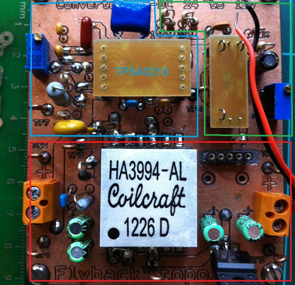
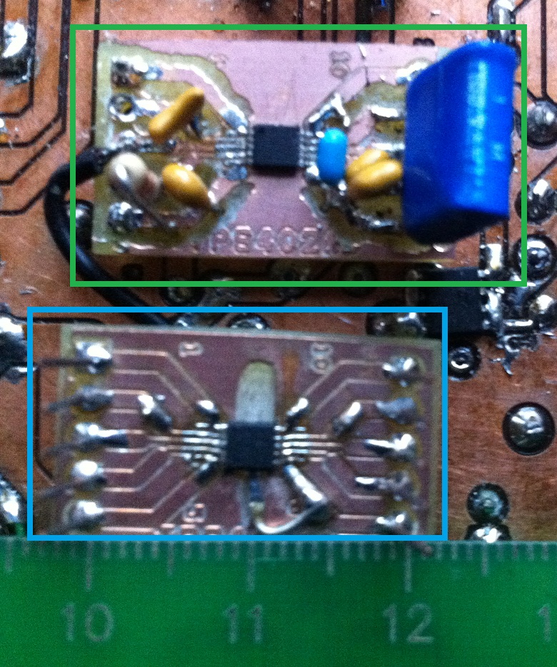
Hello, i mounted PCB with the schematic of application note pmp 2890. This circuit is a flyback converter with TPS40210 as controller.

i´m selected input voltage 24 v for output voltage 12v and load is 45 ohm for output current 270mA.

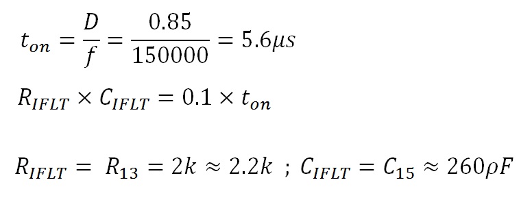
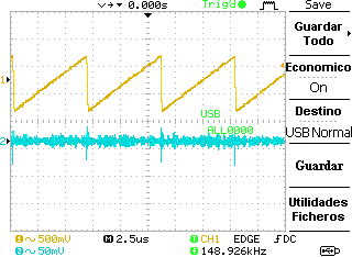
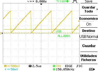
i adjust the switching frequency in RC a 150 kHz.


I have following the datasheet TPS40210, in the gate drive circuit (page 23), i have also replaced Rg. In the original design Rg = 20 kohm but as Qg=24nC in my mosfet,

Rg = 105 / Qg = 105 / 24 = 4,37 ohm

It´s much smaller than the original Rg.

The datasheet also recommended connect the third pin (DIS) a GND.

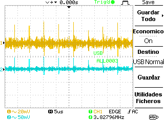
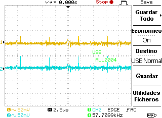
With this changes, and before the changes, output voltage is zero.

This changes are good for the circuit?

i think that the oscillator of TPS40210 don´t started and don´t trigger the mosfet. as I can check? as I can fix it and get the expected output voltage?

Thank´s.

  • Hi Luis,

    The original is 20 Ω (not kΩ) on the PMP2890 schematic so your new resistor is reasonable. Also as you mention DIS should be connected to ground to enable the part. These changes are ok.

    Is the screenshot you have given of the RC pin for this same board? If so it seems like the oscillator is running. Are there switching pulses from the GDRV pin even though there is a ramp at the RC pin?

    Best Regards,
    Anthony

  • Yes the screenshot is in the pin 1 (RC), is the first thing I checked.

    After replacing Rg, in pin 7 (GDRV) i see the screenshot (the yellow line) :


    i don´t know as considered this signal but i think cannot trigger the MOS. I expected a square signal in this pin (GDRV) but I only see that kind of noise and don´t know if correct.

    In the original design use MOSFET Si4484EY but don´t manufactured now, i used his equivalent Si4056DY. The two mosfet are same manufacturer, vishay.

    Thank´s.

  • I continue looking at solutions. Here i will refer to page and equations located at datasheet of TPS40210.

    Reviewing the datasheet for this circuit, in page 12, equation 2, the duty for continuous conduction mode is:

    i don´t know that mean the negative duty.

    And duty for discontinuous mode, page 12, equation 3:

    With these dates in page 16, Current sense filtering equation 11 and equation 12:

    C15 is 260 pF and not 100 pF, i don´t know go for the right track with this calculations.

    Why choose C15=100pF in the original design?

    I see now in pin 1 "RC" (yellow) and pin 2 "soft--start" (blue)

    The signal in this pins are expected, but Vout is zero yet. Another pins doesn´t has signal.

    Where I can continue?

  • are some consideration for the design of the pcb?
    C7 (1uF) is an electrolytic capacitor or ceramic?
    is necessary that C7 is near to controller TPS40210?
    is necessary that C6 is near to controller TPS40210 to generate the soft-start ramp correctly?

    Thank´s.

  • Hi Luis,

    A few comments. The equations in the datasheet apply only to a boost design. The design equations such as duty cycle will change for flyback and depend on the turns ratio of the transformer.

    C7 and C6 should be ceramic and placed near the controller to provide good bypass. You can check the BOM for the reference design to find this. Also the placement of C7 is more critical of the two because it is used to provide the instantaneous charge to turn on the FET and to power internal circuitry.

    For the SS signal in your screenshot, when zoomed out does the voltage never ramp up at all or does it show a waveform similar to Figure 26 in the datasheet? If it is similar to Figure 26 current limit is being falsely triggered.

    Best Regards,
    Anthony

  • ok, then what are the formulas for the design of the application note? exist other document is not in the web?

    My doubts about the capacitors were because it is rare to see a ceramic capacitor 1u value.

    As for the pin 2 SS (soft-start) before was this signal, proportional to pin 1 RC:

    but some times is this signal in pin 2 SS:

    never is similar to Figure 26, I think there is no overcurrent.

    I have checked the connections and components separately, which could be the reason for the overcurrent condition?

  • I still have the test to run the application note.

    I think that i have overcurrent on pin 2 SS 8v. I mounted control part for separated, only the TPS40210 with resistors and capacitors, but the waveforms in the pins are the same.

    There may be an error in the current meter design ISNS pin 7?
    You can facilitate the design equations for the flyback configuration?

    Finally, the TPS4210 is metalic for back part, that part must be soldered to GND (zero voltage)?

  • Luis,

    The following application note could be used as a reference for design equations for a CCM flyback.

    http://www.ti.com/lit/an/slva559/slva559.pdf

    So the SS pin never charges up? Even if the time scale is changed to ms scale instead of µs? Can you check if there is a short from the SS pin to ground? Even in an over current condition the SS pin voltage should ramp up to about 700mV then discharge to about 150mV creating a sawtooth waveform.

  • OK, i prove this changes and don´t found the error.

    The pin 2 SS has 7 V DC, I check with differents capacitors and don´t result.  Don´t short from the SS pin to ground. I don´t see waveform of overcurrent (figure 26 of datasheet).

    The controller TPS 40210 don´t start and i don´t know the reason. I belive the problem is in the soft start, the design has something that cancel soft-start.

    The pin 8 GDRV hasn´t signal, and don´t shoot the gate of MOSFET. As can i that start the controller, is a easy design and has a few pins for prove and i don´t found the error.

    I belive that the controller work because:

         * The pin 1 RC have a correct sawthoot signal.

         * The pin 3 DIS/EN is connect to ground for run the controller.

         * The pin 6 GND is connect to ground.    

         * The pin 9 BP have correct voltage (8v DC).

         * The pin 10 VDD is connect to voltage in 20 V DC.

         * The other pins hasn´t signal.

  • It does sound like the controller is operating but for some reason is not switching. You mention the other pins have no signal. What is the FB pin and COMP pin voltage doing? With no signal are they at some DC voltage or are they at GND?

  • ok, the voltage in pins are:  

         * The pin 1 RC have a correct sawthoot signal between zero volts and VDD/20 volts. 

         * The pin 2 SS have 7,3 volts DC.

         * The pin 3 DIS/EN is connect to ground for run the controller.

         * The pin 4 COMP have 700 mV DC without signal in output converter. If i simulate 12v DC in output converter, that is expected if run properly, i measure 1,4 volts DC.

         * The pin 5 FB have 700 mV DC too. If i simulate 12v DC in output converter, that is expected if run properly, i measure 8 volts DC.

         * The pin 6 GND is connect to ground.   

         * The pin 7 ISNS 180 mV DC. If i simulate 12v DC in output converter, that is expected if run properly, i measure 2,7 mV DC.

         * The pin 8 GDRV 0.1 mV DC, i understand that zero volts.

         * The pin 9 BP have correct voltage (8v DC).

         * The pin 10 VDD is connect to voltage in 20 volts DC.

    Thank`s for your help, Luis.

  • Thank you for sharing the details at each pin. Please see my comments below. For these three pins it would be better to see an oscilloscope screenshot instead of a DC measurement. This can give us an idea of the behavior at these pins. Can you also share how you are simulating a converter which is running properly?

    * The pin 4 COMP have 700 mV DC without signal in output converter. If i simulate 12v DC in output converter, that is expected if run properly, i measure 1,4 volts DC.

    700mV tells me that the part should not be switching. The valley voltage is 1.2V typical so the COMP voltage must be greater than this in order for switching to occur. Is there a short from FB to COMP?

    * The pin 5 FB have 700 mV DC too. If i simulate 12v DC in output converter, that is expected if run properly, i measure 8 volts DC.

    When running properly the FB voltage should be 700mV DC. The controller will try to regulate the FB voltage to the internal 700mV reference by adjusting the COMP voltage.

    * The pin 7 ISNS 180 mV DC. If i simulate 12v DC in output converter, that is expected if run properly, i measure 2,7 mV DC.

    If ISNS is 180mV DC this would indicate an over current. The overcurrent detection threshold is 150mV typical. If the device is not switching, I am curious how a voltage is measured at the ISNS pin. This means there is approximately an average of 1A of current going through R18.

  • Hi, i note your considerations.

    Can you also share how you are simulating a converter which is running properly? I have not gotten it to work yet.

    Is there a short from FB to COMP? not, but only separate for 2.2 Kohm resistor in parallel with a 33pF capacitor, as shown in the design.

    I am curious how a voltage is measured at the ISNS pin. This is my test circuit:

    I don´t have smd components, i build this PCB for application note with PTH components


    In red the power part, in blue the control part and the feedback in green part.

    The measures with multimeter are in each pin.

    The only one error can be the dimensions, is a little big  but i don´t found the error.

    For these three pins it would be better to see an oscilloscope screenshot


    For pin 1 RC and pin 2 SS, You can see the soft-start don´t work. I believe as has overcurrent, activate OC fault and don´t work the controller, but i don´t know as remove this error.

    For pin 4 COMP and pin 5 FB, the peaks are repeat qith 150 kHz more or less

    For pin 7 ISNS and pin 8 GDRV

    The other ins has signal without waveform.


    As I can solve the problem with overcurrent?

    I can remove the overcurrent measurement and protection?


  • The layout is likely the source of your issues. Using this method for prototyping may be quicker and easier but introduces so many additional factors which can cause problems. The connections to the TPS40210 pins look very long which adds a lot of inductance. The increased inductance makes the part extra sensitive to noise. Is it possible to see the layout of the PCB near where the TPS40210 board is soldered onto it?

    Also the peaks being measured on these signals is likely noise from the RC ramp. The peaks line up with the falling edge of the RC waveform.

  • Also the peaks being measured on these signals is likely noise from the RC ramp. The peaks line up with the falling edge of the RC waveform.

    Yes, the peaks coincide with the slope of the sawtooth signal.

    Is it possible to see the layout of the PCB near where the TPS40210 board is soldered onto it?

    Yes, of course. I chose to mount the controller TPS40210 on a pcb  extra because being so small I had troublewith the solder without breaking the PCB.


    In blue, the pcb with which I have done all the tests. In green the pcb modificated with capacitors very near of the pins.

    With modificated pcb (in green) for controller has lower noise but in pin 4 COMP and pin 5 FB has 700mV DC more or less. In pin 7 ISNS has 10mV DC before, (with blue pcb) has 180 mV.


    Any recommendation for pcb controller, or the capacitors are sufficiently near?


    Tomorrow probe more changes. I will mount parallel capacitors to lower parasitic inductance and prove new pcb.

    I hope to solve the problems.


    Thank´s, Luis.


  • Hello, the recurring problems, and I'm still working on that work correctly. Still no pulses at pin 8 GDRV.

    After see the pcb and how are near the capacitors, would be enough to make it work?

    The only significant change in the schematic of the application is the transformer, I chose the reference HA3994-AL of coilcraft to have similarly inductance. Datasheet attached for you to give me your opinion.

    If is this the problem, i have also avaliable other references:

    FA2901-AL
    FA2900-AL
    JA4590-AL
    JA4637-AL

    What would be the more convenient?

    6165.HA3994-AL.pdf

    3108.FA290x-AL.pdf

    0456.JA4590-AL.pdf

    6404.JA4637-AL.pdf

    Thank´s, Luis.

  • Hello, one more idea for work this circuit?

  • Hi Luis,

    The best recommendation I can provide is to duplicate the component selection from the bom and the layout of the PMP2890 as close as possible first. The new components and layout introduce so many factors for a switching power supply making this very difficult to debug. It is best to start from a known working design.

    I have attached the layout of this board for your reference. It is in PCAD and you can find a viewer to open it by searching online.

    6404.PMP2890_Rev_A.PCB

    Best Regards,
    Anthony