This thread has been locked.

If you have a related question, please click the "Ask a related question" button in the top right corner. The newly created question will be automatically linked to this question.

Note on the document SNVA532 Buck Converters Provide a Battery Charger and System Power

Other Parts Discussed in Thread: LMC7101

Dear All,

I've found this very nice document about battery management with a Buck DC-DC acting as a current-source and voltage source for charging a battery.

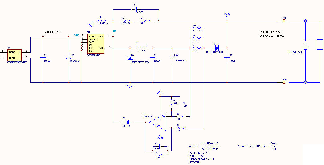
I'd like just to signal a probable mistake into the circuit behaviour on page 2 of the document. The U3 is a differential amplifier connected to amplify the voltage across the sensing resistor R5. Due to the connection of the differential amplifier U3 the output voltage is directly proportional to the current flow trough the sensing resistor and not, as written, inversely proportional. In this way when the current trough the resistor R5 take a value able to produce a output voltage greater than the reference voltage that is inside U1, the feedback loop reduce the U1 output voltage then the current trough the load and battery. When the current request from the load is lower than the programmed value (set by the value of R5) the U3 output voltage is lower than the voltage supplied from the resistor divider (R2 and R3) then the diode D2 will be inverse polarized hence not able to conduct. In this situation the current loop is not working and the feedback came directly from the resistor divider hence the regulator work as a voltage regulator.

Hoping to have explained in a clear manner the circuit behaviour your comments are welcome.

Best regards

Fabio

  • I have forwarded your comments to the original author.

  • From the original author:

    "You are correct.  The output of the regulator U1 is inversely proportional to the current across R5 (when in constant current mode), but as stated the output of the op-amp U3 is directly proportional.  I will see if we can have the word “inversely” removed from the text.

    Thanks very much for your feedback!

    Bob Hanrahan"

  • Thank you Bob for your reply.

    I've a nice update, after reading the paper I decided to make in practical the charger in order to charge a NiMeH battery pack of 4 elements (each battery is a 2000 mAh AA style).

    Nominal output voltage was programmed to 5.5 V and output current was limited to 300 mA.
    This battery charger must feed the batteries pack and also supply a circuitry which can be viewed as a parallel load to the batteries with a supply current of approximatively 100 mA.

    What I want to examine in detail is the behavior of the controller when it works as a constant current generator.

    Here I've attached the schematic drawing, the pcb photo and some waveform taken in a working pcb during the charging stage (the batteries pack was previously fully discharged).

    This is the files description:

    - CHARGER.jpg this is the photo of the PCB

    - SCH.jpg: the circuit schematic

    - Fig1.jpg: referring to the schematic the VA_D3 is the voltage on the Anode of the Diode D3, likewise the VU1_8 is the voltage on the output of the LM2594ADJ buck controller.

    -Fig2.jpg show on the top figure the output voltage taken on the batteries pack, the bottom trace show the burst on the output pin of the buck regulator.

    - Fig3. jpg the top trace show in detail the output voltage that we've at the output of the differential amplifier U2 (LMC7101), this voltage has a offset of 1.5 V and into the figure, at the bottom part, are shown the max, min and avg value as measured by the digital scope; the bottom trace is the voltage on the output pin (pin 8) of the buck controller U1.

    From all the figure I can suppose that when the current loop taken precedence over the voltage loop the switch regulator will be opened and the regulator at the end fall into a DCM mode (the inductor discharge have a constant di/dt), when the current goeas below the trip limit the voltage loop mode take control and then the buck regulator behaviour take to act as a classical CCM mode. In this stage the regulator behaviour is a sort of bursted CCM with a small DCM mode.

    After some time, when the overall current supplied to the load (battery + load) goes below the threshold current point the behaviour will be always CCM until the current take goes below a value that make the regulator in DCM mode.

    Here is my first evaluation about this circuit, it looks cold and work nicely, but I like to get more information and theory about it then I hope you can give me some feedback on it.

    Best regards

    Fabio