This thread has been locked.

If you have a related question, please click the "Ask a related question" button in the top right corner. The newly created question will be automatically linked to this question.

LM3150 DCDC 12Vin ->3.3Vout 8A, oscillation in SW pin

Other Parts Discussed in Thread: LM3150

Hi,

We have implemented a webbench design, based on LM3150.

It's a 12Vin, nominal, to 3.3Vout  8 A.

It powers a highly capacitive load (8x 680uF tantalum capacitors)

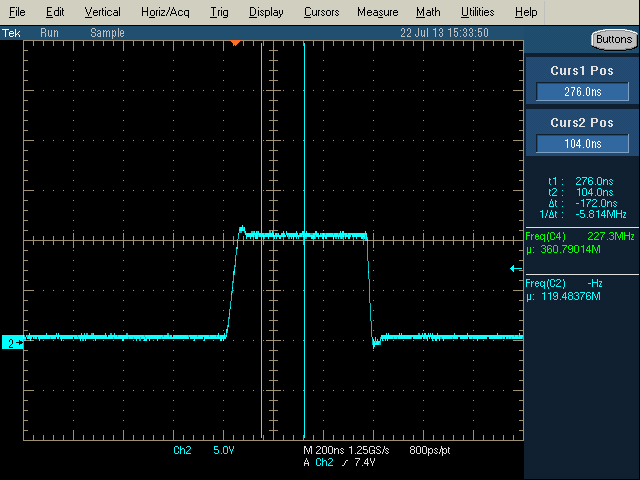
When I look at the voltage at pin SW, with almost no load (some logic plus the 680uF capactiors), we see a clean step waveform

But when we apply any load (by the moment a resitive load, plus 680uF capacitors), we can see some kind of oscillation, that we think it doesn’t be there
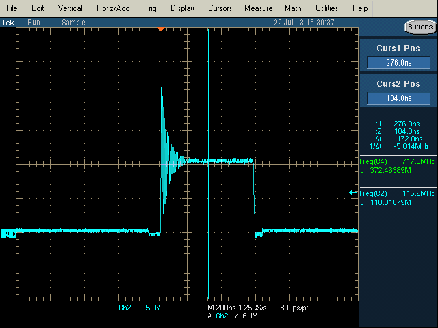
 

And zoomed

I use the webbench part numbers, excep for:

* Cin. I have two additional CAPs ( 100uF 25V electrolitic aluminium) before Cin.

* Css. I have changed Css to 1uF to slow down the ramp-up.

* Cout. I use two 680uF 6v3V in parallel befor plane conection (0.6 ESR each).

Is this oscillation undesirable?

any clue on what is causing this oscillation?


thanks

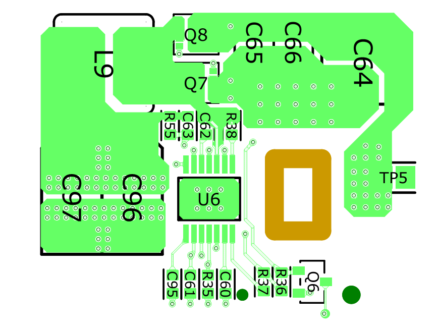
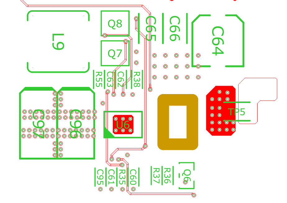
PD.- the webbench desing:

5852.Report webbench 8-18Vin 3.3Vout 8A.pdf

  • Hi Daniel,

    Let me forward your applications question to the Apps engineer in charge of this product and he'll get back to you shortly.

    Best Regards,

    -Juan

  • Hi Daniel,

    You will usually see some ringing on the switch node.  In many cases the ringing won't cause any problems.  However, excessive ringing can sometimes effect EMI performance or be a sign of layout or noise problems.

    Possible causes

    1)

    The ground loop on your scope probe might be too large and the fast transition of the node is causing ringing.  Try a shorter ground loop or pig tail. 

    2) 

    Excessive ringing can also be a sign that the ceramic input bypass capacitors are not close enough to the power stage or need to be increased.  Look on your layout and see how close the input capacitor is to the drain of the high side fet and the source of the low side fet.  Any extra inductance in this loop will cause ringing.  Post your layout and I will take a look.

    3)

    The fet you are using might have a very low gate charge and turns on very quickly.  With Qg less than 10nC the transition speed of the FET as it turns on might be very fast.  The fast turn on will cause the Cds capacitance of the low side fet to ring with the stray inductance.  If this is the cause you can either add a snubber.  (Add a capacitor from the switch node to ground until the ringing frequency is four time lower,  Then add a small resistor in series to absorb the energy).  Or you can try to slow down the transition speed of the fet by addind a 1-10ohm resistor in series with the high side gate.  This creates an RC filter with the fet gate capacitance.  You should place a diode anti parallel to the resistor to make sure the part can still turn off the gate quickly.


    Hopw this helps,

    Marc


  • Hi Marc,

    This is the actual schematic for our DCDC:

    and the corresponding layout:

    TOP layer

    and Bottom layer, with TOP components outlines superimposed:

    It's a four layer board, but L2 is GND plane and L3 is +3.3V + 12Vin planes.

    I made some test with your sugerences and these are the results.

    1) Oscilloscope ground loop. I had improvised an oscilloscope PCB adaptes and measured V in SW pin betwen R28 an the near ground plane. This, i think, results in almost no ground loop. I can see the same oscillations in SW voltaje.

    2) Far or low Cin. My Cin is conformed by c61 (100nF 25V 0603), C65 and C66 (10uF 25V 1210, part number AVX 12103D106KAT2A)  and a bulk alluminium capacitor.

    I had soldered two aditional 10uF caps, literally above C65 and C66, and seen no change.

    3) A) add a snubber. I tryed some caps until Oscillation frequency is four time lower. This Cap was 10nF, then add in a series resistor (i tried 2 Ohm)

    It works but, i think it consumes too much power. If i am correct it is:

    P = C* Vin^2*freq = 10e-9* 144* 500e3  = 0.72W

    3) B) add a 1-10 Ohm resistor in series with Q8 gate to slow down the transition. I tried a 10 Ohm resistor with no apreciable change in the oscillation.

  • Hi Daniel,

    A quick look at your layout.  It looks pretty good.  So I think we can rule out ground loop and layout as primary causes.  That leaves us with a very fast turn on of the FET.

    Let's try two things.

    1)  The ringing frequency is around 120Mhz.  Can you place an 1000pF 0805 COG ceramics capacitor on the input as close as possible to the FETs. Place it to the left of C65.  This cap will have a resonant frequency around 130Mhz and it might with the ringing.

    2) There is a higher QG version of the FET the CSD17304.  This should have a slightly slower turn on speed and might reduce the ringing.  


    Also you could try reducing the snubber capacitance to save on the power consumption.  This will be a balance between the power dissipation you can accept and the ringing. As I said before, some ringing is acceptable as long as the part is regulating correctly.


    Regards,

    Marc