


Hi,
I am using the LM2663 to provide a negative power rail from a +5V supply. This is then passed through a -4.5 LDO regulator to create a create a clean negative rail for sensitive op-amps and ADC/DACs. My problem is that, due to my current board layout, the LM2663 is injecting large currents into the ground/power planes that are corrupting signals in the sensitive analog components on my circuit.
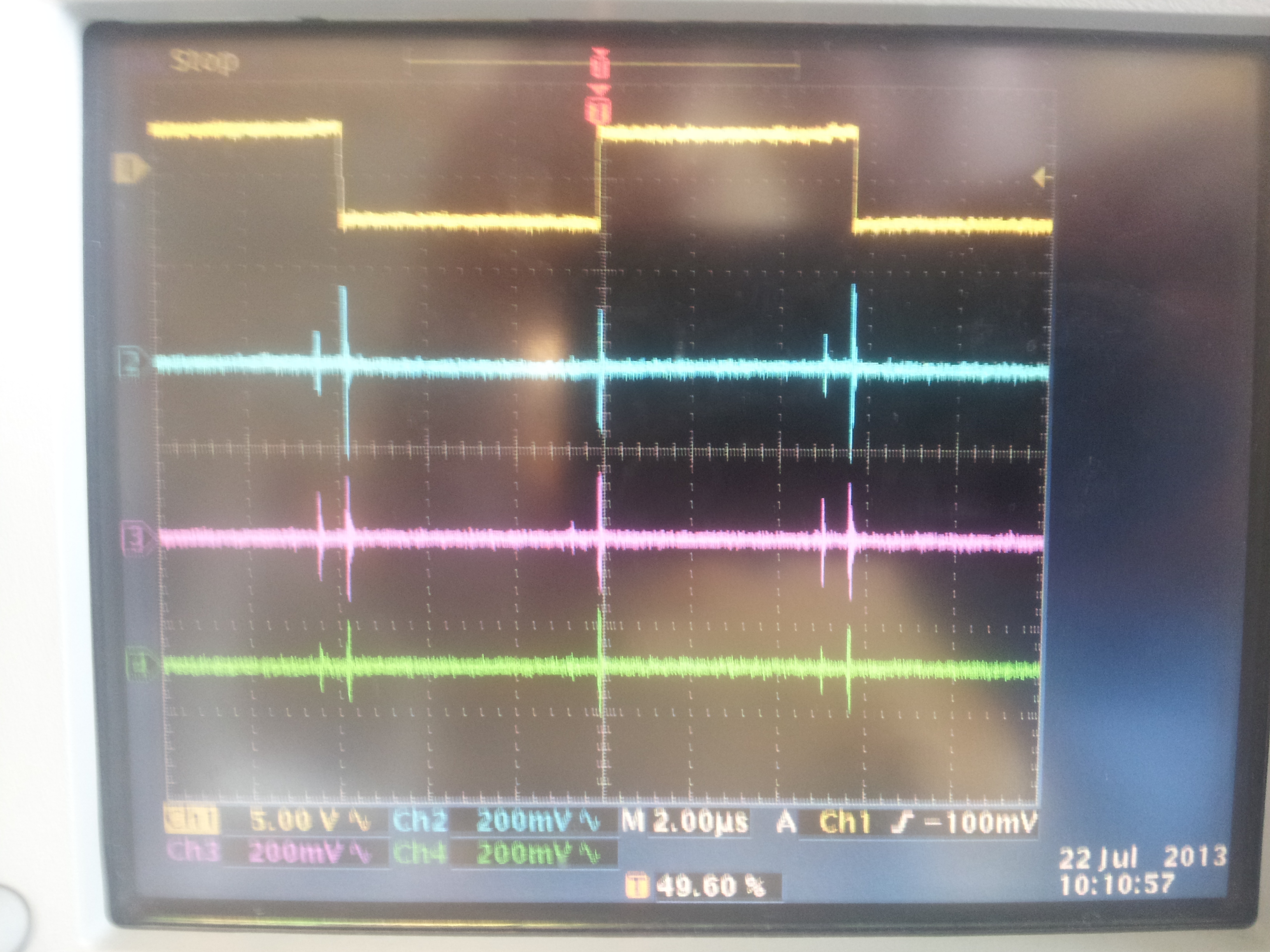
Here is a picture of the problem (Yellow: Positive terminal of charge pump capacitor for the LM2663, C32 in schematic below, Pink: Vout of LM2663, Blue: Negative rail after regulation by MAX1732, Green: Positive rail after regulation byTLV70245. All measurements referenced to AGND)
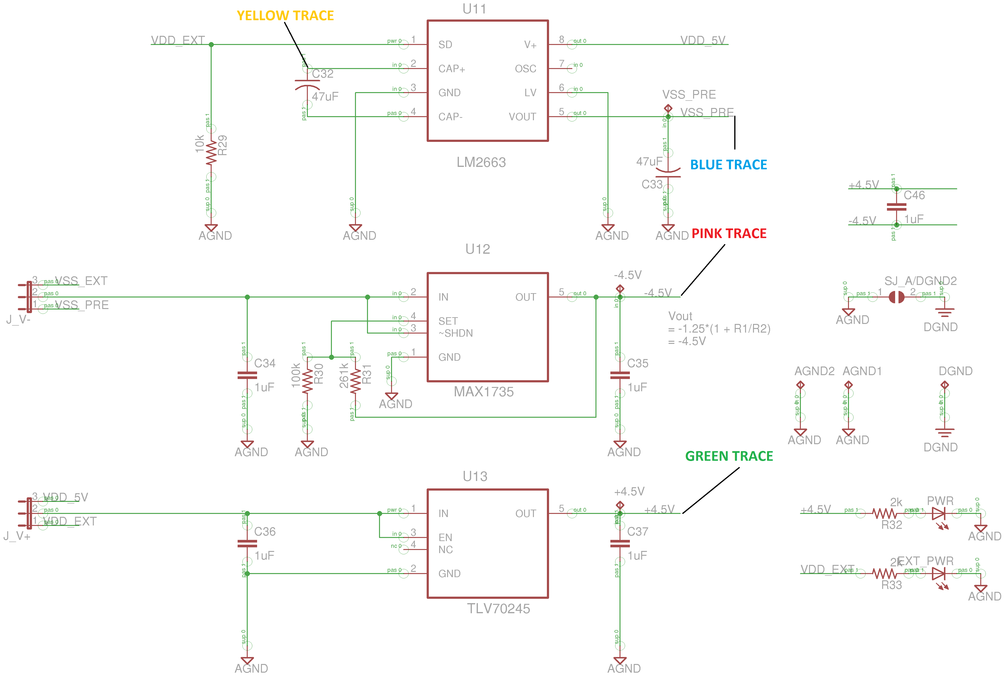
Here is a schematic of the circuit that shows the locations of the test points in the figure above:
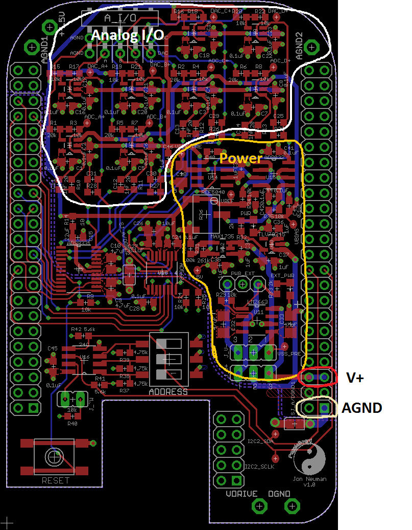
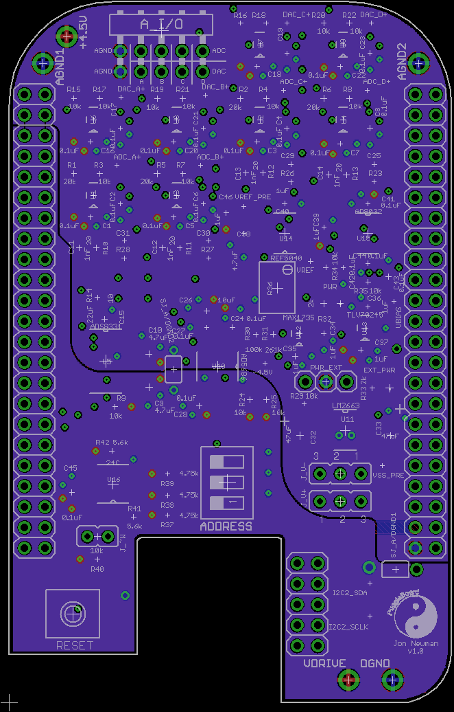
Here is a picture of my board, with power and analog sub-systems circled:
Here is a picture of the LM2663 layout, and corresponding schematic, that might indicate why I'm getting these voltage spikes.
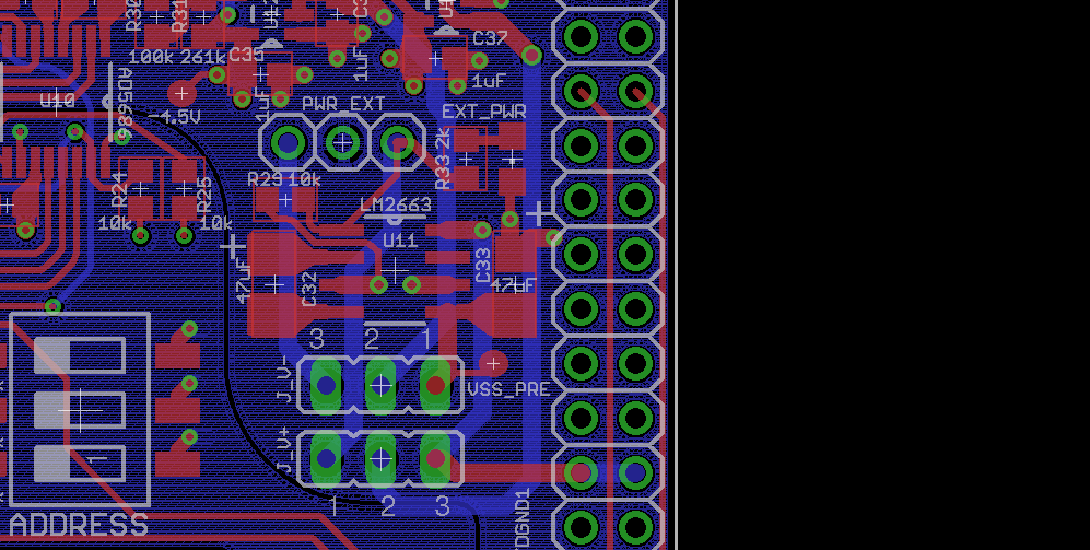
This is a 4-layer board. It has an analog ground plane and a positive supply plane, which overlay (blue area in figure below.) The second planes to the left of the board are the digital supply and ground planes. The negative rail does not occupy a copper plane, but is transported by thick traces. I note that the charge pump and output capacitors are laying over the ground a power planes and I wonder if they are capacitively coupling into the planes.
Any advice on improved layout, component selection, etc in order to stop these voltage spikes from corrupting the ground a power rails of the system would be great. Thanks for your help.
- Jon
