Dear all,
I am developing a specific power supply based on LM5030 and I would appreciate some help.
The supply is a push-pull configuration, ~non-isolated, 9-16VDC nominal (8-18V "should work") input, multiple outputs (+9.5VDC; -9.5VDC; 6VDC; 10.6VDC), total power of ~4W maximum, the basic criteria is a very low noise -> so it must be synchronizable (will power precise synchronous detectors and ADS1281 ADCs...)
The load on the outputs is supposed to be quite stable but anyway, there is a common output choke to improve regulation of the "non-sensed" outputs. The feedback goes from the 10.6VDC which is supposed to deliver highest power (0.5-1W). I would also like to get some "reasonable" efficiency; the device will be powered from accumulator in some cases... The price or complexity of the circuit is not an issue; the low noise is the main criteria.
Please check the circuit. Now I have placed on PCB everything with the exception of stabilizers U2, U6, U9, U7. The circuit is loaded with some fixed value resistor, actual power is 2.3W.
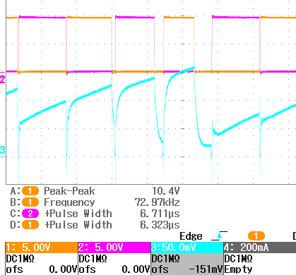
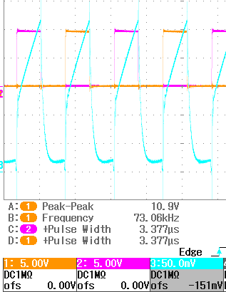
The circuit basically works, but sometimes for some input voltages, there are some hf oscillations - the IC switches at ~2MHz speed instead of 75kHz (150kHz input synchronization signal). The oscillations are not stable, you can here a modulation in acoustic frequencies..., the input current increases and transformer gets hot...
I am not pretty sure about the values in the compensation C46,C47,R22 - I took them from some similar (but higher power) example on TI website. Also not sure if U11 (common mode choke) can cause some troubles. I tried to place D7,D8 but it did not improve anything and I prefer to have slower edges to have lower noise.
Basically the circuit works better when there are standard 10:1 oscilloscopic probes connected to the gates of U5 mosfet. Or the oscillations can be influenced by touching the PCB close to the control IC... The PCB has two layers now, with a solid ground-plane on bottom, the PCB will be 4-layer later. I think I have some experience with PCB design, this should be OK.
The transformer is a ferrite toroid based (16mm diameter) u=2100, Bmax calculated ~50mT... should be OK, as well as the U1, which is MPP core based and has the same number of turns as the secondaries of the main transformer. I am a newbie in the switched supply design so maybe I did some elementary error.
Thank you for any suggestions
Vojtech