This thread has been locked.

If you have a related question, please click the "Ask a related question" button in the top right corner. The newly created question will be automatically linked to this question.

TPS2410 Problems

Other Parts Discussed in Thread: TPS2410, TPS2412

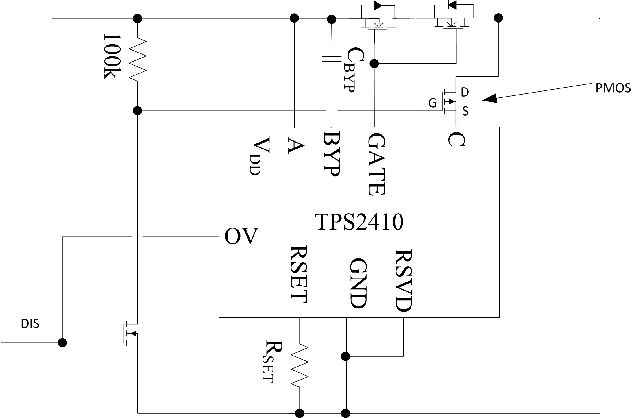
My customer is having a problem with the TPS2410 (see attached schematic).


The ideal diode functions as expected and is used as a bidirectional current control.

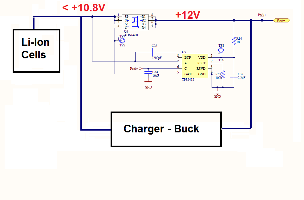
The 12V bus is connected to the C pin as per page 22 of the spec sheet (Bidirectional control and blocking).

The issue with the device is when the ideal diode is disabled.

Signal BBU_ENABLE_L is active low, 12V bus goes low  and VBAT1 (battery voltage) is 15-20V.

No power can be pulled from the battery but a voltage is measured on the 12V bus in the order of 3V.

The customer is monitoring the 12V bus. If there is a voltage, the host assumes the 12V bus is ok.


What can be accomplished to remove this voltage on the 12V bus?

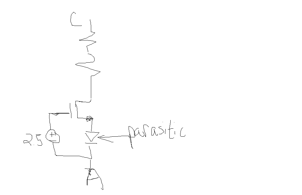
The voltage is leaking from the resistance between the a and C pins on the controller.


Here are testing results. The C-pin current is way outside of specification. The total current is not accounted for (IN = OUT). It appears that Vac ~= -1.8V is a threshold for sourcing/draining current from the A-pin.


Test Name

C-Voltage (V)

A-Voltage (V)

A-Pin current (uA)

C-Pin Current (uA)

GND-Pin Current (uA)

Comment

Voltage Delta (External - Cell) (V)

Minimum PS-V #1

11.64

7.2

-530


A pin charges the cell stack

4.44

Minimum PS-V #2

10.11

77


A pin discharges the cell stack

1.53

Minimum PS-V #3

10.44

176


A pin discharges the cell stack

1.20

Minimum PS-V #4

10.65

245


A pin discharges the cell stack

0.99

Nominal PS-V #1

12.20

7.2

-566

1225

3074

A pin charges the cell stack

5.00

Nominal PS-V #2

10.11

-88

1225

2999

A pin charges the cell stack

2.09

Nominal PS-V #3

10.44

12

1225

2985

A pin discharges the cell stack

1.76

Nominal PS-V #4

10.65

88

1225

2977

A pin discharges the cell stack

1.55

Maximum PS-V #1

12.36

7.2

-570


A pin charges the cell stack

5.16

Maximum PS-V #2

10.11

-135


A pin charges the cell stack

2.25

Maximum PS-V #3

10.44

-36


A pin charges the cell stack

1.92

Maximum PS-V #4

10.65

28


A pin discharges the cell stack

1.71

  • David,

    You are correct there will be a leakage current of roughly 1mA towards the output. If the bus has no load it will float up as you notice. You have 2 options:

    1) Add a dummy load of 1k-ohm on the bus.

    2) use 2 logic FETs to disconnect C from V_bus when the ORing controller is disabled. As shown in the diagram below.


    As a side note, you never posted the attachment.

    -Artem


  • Sorry the polarity on that diagram was not right. Please refer to the one below:

     -Artem

  • Hi Artem,

    The responses here focus on leakage through the C pin. My concern is leakage through the A pin. When Vac <= roughly -1.8V, electrical current flows out of the A pin. It appears that the feed for this current is through the VDD pin. 

    My application is a OR-ing control on the output of a lithium-ion battery pack. The charger circuitry is on-board the battery pack, and placed in parallel with the output OR-ing control. The typical state of the TPS2412 is to have +12V available on the C pin, and cell stack voltage on the A pin (+10.8V when charged, for this pack). When the charger is disabled, the cells continue to charge due to leakage through the A pin. This charging is on the order of ~600uA worst noted case, to a voltage equal to C voltage (+12V) - 1.8V. 

    If you view the data table found in the original post, you will see this issue in record. 

    Please recommend a workaround or supply a specification for the A pin leakage characteristic.

    Lucas

  • Lucas,

    Could you provide a schematic. I want to make sure that I understand how everything is hooked up.

    -Artem

  • Hi Artem,

    Please update your progress recommending a workaround or supplying a specification for the A pin leakage characteristic

    Lucas

  • Lucas,

    Sorry for the slow response. I was out on vacation.

    You mentioned that the C current was outside of the Spec. Are you measuring the C and Vdd current or just the C current.

    With the A current, are you concerned with A sourcing current and charging the battery? 600uA is mainly a residiual of the charge pump. It seems pretty harmless... If it's a big concern for you, you can hook up Vdd to the A side instead of the C side. Vdd will always sink more current than A sources so you should be okay. Another alternative is to hook up the circuit that I drew up previously on the C pin.

    - Artem 

  • Hi Artem,

    Thank you for your response. 

    The C pin was lifted and an ammeter was used to measure the current flow. The voltage of A was kept below the voltage of C. The test results are provided at the top of this forum post. The C current was consistently measured as 1225uA. The specification states a maximum of 10uA on C when Vac <= 0.1.

    The leakage of the A pin is a concern when this TPS2412 device is used in energy storage devices. 600uA may seem small, but after a time duration the energy accumulation is non-negligible; the leakage path effectively functions as an unregulated charging source. Excessive energy injection into an energy storage device is a major concern.

    I will evaluate the VDD->A pin suggestion.

    Lucas

  • Lucas,

    I understand your concern. I am a little surprised by the current on C being ~1.25mA.  I will check this with the designer and dig into how big the sourcing current on A is supposed to be.

    In terms of a work-around hooking up A to Vdd or adding a "dummy load" with a series FET (driving by the OV/disable signal) are the best I can think off.

    After thinking it through I don't think that disconnecting C from the source of the ORing FET is a good idea, b/c the charge pump voltage is derived from A and it needs to be tied to the source.

    -Artem

  • Hi Artem,

    Long term analysis of our current solution (with A pin providing charging energy) indicates that the cell stack voltage will reach steady-state at approximately 1.8V under the voltage found on the C pin. If the cell stack voltage is within approximately 1.8V of C pin voltage, the A pin will drain energy from the cells.

    Please make inquires with you team to determine if this threshold will hold across all TPS2410 parts, and with what tolerance. The expected application voltages for C pin are found in the first post of this thread.

    Lucas

  • Hi Artem,

    Please respond or provide another means of gaining application support from Texas Instruments. 

    Lucas

  • Lucas,

    I though that you were going to connect Vdd on the A side like I suggested. Vdd will always draw more current than what A supplies and you should be fine. Were there issues with this solution?

    With regards to your question about the A pin sourcing current, unfortunately this wasn't something that was characterized.  This part was primarily designed for applicaitons with a single FET, where this isn't a concern. I understand how in your application this is a big deal.

    -Artem


  • Hi Artem,

    I can see where this thread is a bit confusing. The initial poster of this, David Schmidt, was providing distributor support for a different issue (we use the TPS24xx part in multiple projects) and listed my test results with the description text of the other issue. That other issue is actually current leakage from C pin, and was mitigated by adding the dummy load suggested. 

    The issue I am chasing is captured in my posts (and the test results provided by David correspond to the issue I am chasing).

    Please reference the schematic provided in this thread. This is a single NFET application. The A pin leaks current through the ideal diode controller in proportion to the voltaic difference between A and C. 

    The issue with tying VDD to A pin, is that performance of the part is not specified when voltage is applied to C pin, without VDD being powered. Our application will spend large period of time with a voltage on C pin and A pin (therein also VDD pin) floating/undriven. We see this as an increased risk to the TPS24xx chip and chose not to take this approach.

    Please provide a TI contact who can support characterizing the nature of the voltaic proportionality seen between A and C, with respect to current magnitude sourced from the A pin in direction opposite the ideal diode intent.

    Lucas

  • Thanks Lucas. This makes more sense now.  This behavior is not consistent with how I would interpret the spec. Let me get some data on the EVM and ask design.

    -Artem

  • Lucas,

    I collected the following data on the EVM, which seems to be in line with what you were saying. Negative I_in means that A is sourcing current.

    Vin (A) Vout -  C I_in 
    0 12      -1.3mA
    6 12      -0.97mA
    10 12      -81.9uA
    11 12     190uA
    12 12     345uA
    15 12    986uA

    Also we identified the leakage path in silicon.  Still working on estimating the tolerance would be. Voltage on the Vgs of the Vg of the FET is 2.5V.

  • Hi to ever one,

    I want to use TPS2410 to be connected to two power supplies to get the single output..Connecting the two power supplies to a common bus.

    Input sources are  two 12V,10A..

    I didn't find any information of the max input current to the TPS2410..

    Will you provide any circuit or details, about the TPS2410 to interface to the two power sources ..

    Awaiting your reply...

    Thank you!!!

  • Hello,

    Can any one tell me what is the maximum input current for TPS2410..

    In the datasheet mentioned ,driver pin will sustain up to 1A current..

    I want to use TPS2410 as Oring circuit, to connect two power supplies of 12v,10A for redundancy of the power supply.....

    Awaiting your reply....

    Thanks in advance.....

    Lakshmi