Dear TI forum members,
We are experiencing a strange problem with a power supply build around the 54620. As you can see in the (slightly) redacted schematics; components with a *1 next to them are DoNotPlace, and are not present on the boards. 2821.Supplies.pdf we are using 4x a tps54620 and only one of them 3v3 regulator exhibits this problem.
The power distribution network is as follows:
Vbat (24V) to 12V; 12V to 3V3 and 5V; 5V to 1V2 and 1V9
The clock frequency designed as 200kHz (measured as 220kHz) is generated from a separate 3v3 linear supply (3v3_lin).
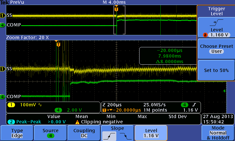
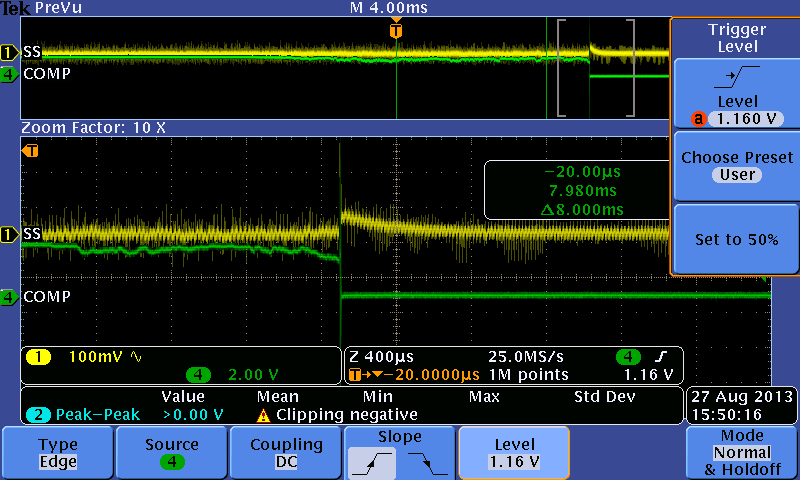
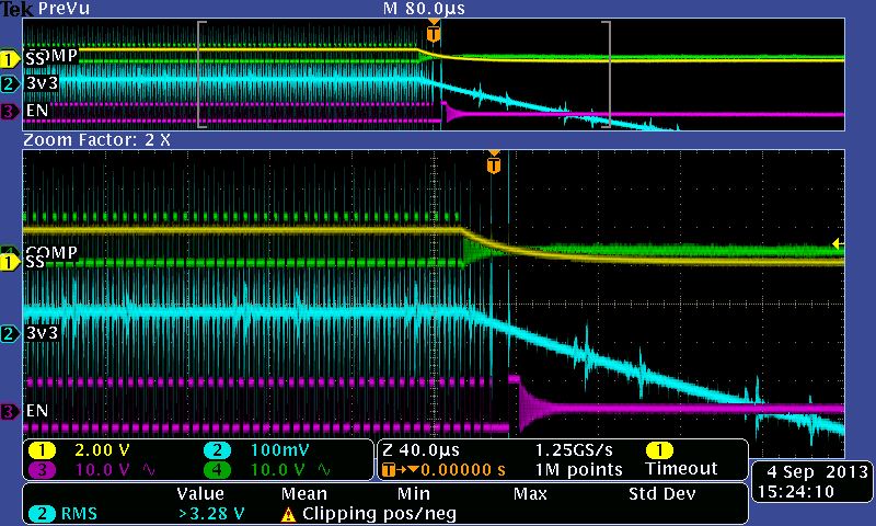
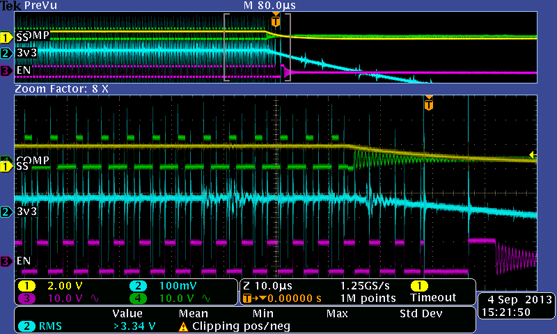
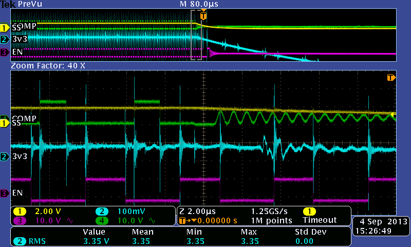
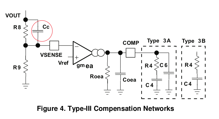
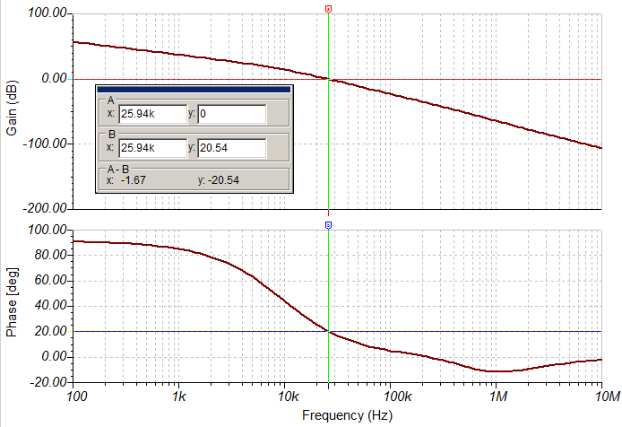
We are seeing the spontaneous shutdowns and restart with ~40% of our first production series. Symptoms are the SS/TR pin going down to zero, Powergood going low, 3V3 dropping to zero, and starting slightly later the 5V also drops to zero (they share the same SS capacitor). Of course we have checked the EN pin for spikes, and also removed IC101 and led D11 so that the 12V_PGOOD net is floating, and have confirmed during a shutdown that the EN-pin does not drop below 2.5V (steady state 3V). The shutdown does not happen after a specific time, although order of magnitude differences seem to exist between different boards. After we replaced the 3V3 regulator on a board which repeatably shutdown within 20min, the board now takes up to 40 minutes or more to shutdown. We have confirmed the loop stability by adding and removing a 3A load. The 3V3 supply has a type III compensation network, with an intended cross-over frequency of 70kHz. The chip stays hand warm.
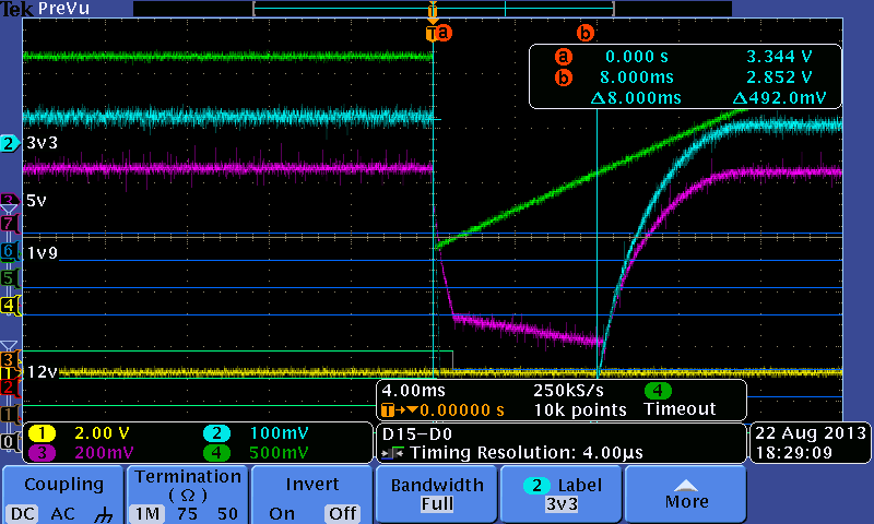
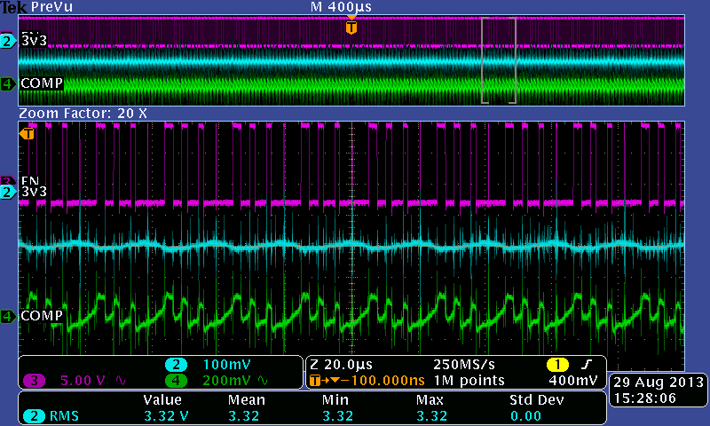
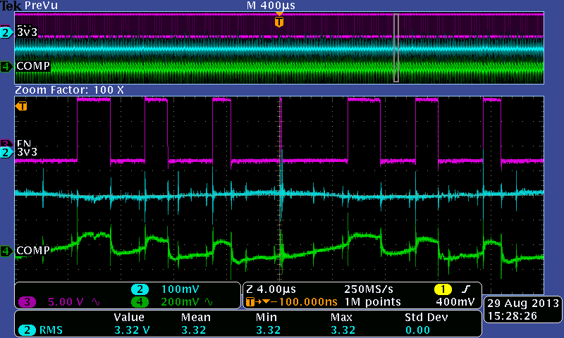
blue: 3v3 with -3.3V offset purple:5v green: SS/TR
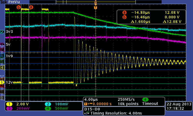
blue: 3v3 with -3.3V offset purple:5v green: SS/TR yellow: PH output of 3V3 regulator
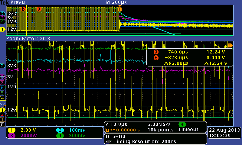
blue: 3v3 with -3.3V offset purple:5v green: SS/TR yellow: PH output of 3V3 regulator
According to the datasheet the only reasons for shutdown are UVLO on VIn (only 200mVpp ripple on 12V), thermal shutdown (only hand warm), or EN pulled low (scope does not trigger with negative going threshold at 2.5V). So something else must be triggering the shutdown.
After removing C391 (3V3 output to V_sense of 3V3 regulator), the shutdown did not happen for the next 2.5 hours. During this time we also confirmed the loop stability using the same 3A load-step test described earlier.
Might it be that our large inductor and low clock frequency together with using the TPS54620_TPS54XXX_App Note_calculator_Ver5p0.xls sheet leads us to a problem only occurring with the 3V3 supply?
Questions:
1: How is it possible that the spontaneous shutdowns seem to be linked to the type III compensation
2: Allthough the maximum rating for the EN pin is 6V, the datasheet suggests only using open-drain buffers to control this pin. Is it a problem to use a 3V3 push-pull buffer?
3: Is it a problem to connect to EN pins together as we have done?
4: Any other problems with the design or visible from the scope images?
Any help appreciated, highest regards,
Marijn