This thread has been locked.

If you have a related question, please click the "Ask a related question" button in the top right corner. The newly created question will be automatically linked to this question.

TPS62110 small signal model for frequency compensation available?

Other Parts Discussed in Thread: TPS62110, TPS54620, TPS62140, TPS62160, TINA-TI

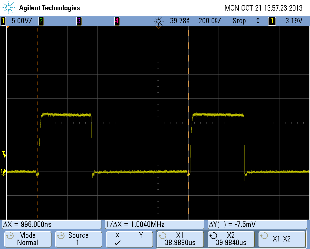
Is there a small signal model available for frequency compensation for the TPS62110?  For example, TPS54620 has a small signal model for frequency compensation on page 20 of its data sheet.

Also, is it possible to increase the frequency of the TPS62110 internal saw-tooth generator?

Thank you.

Regards,

Eric Hooker

  • There is a simulation model on the TPS62110 product page.  It is not possible to change the oscillator frequency but you can sync it to a clock.

    But I would recommend looking at a newer device, such as TPS62140 or TPS62160.  These devices also switch faster.

    Can you share details of why this is important?

  • Chris,

    Thanks for your quick reply.  Does the model on the product page work for other spice simulators or only TINA-TI?  I would rather not spend the time to learn TINA-TI now if possible.  Also, is the model good for transient and linear simulations (gain & phase margin)?

    Also, I measure about 20 mVpp ripple on the output (across Cout caps) at a freq of about 16 kHz -- is this expected?  If so, why does it repeat at a16 kHz rate?  Is there a way I could increase this rate?  The shape of the ripple looks like figure 13 on the data sheet.   My load current is 500 mA, and I supply a 1 MHz clock to the SYNC pin.  The inductor is a Coilcraft 6.8 uH (XAL4030-682ME, DCR =0.052 ohms max) and the output caps are two 22 uF, 10V ceramic X5R caps.  The output votage is 4V.

    Thanks,

    Eric

  • The models forum can help you with the model for any device, including the TPS62110.

    But you have an apps question about the output ripple.  You need to look at the SW node and output ripple to understand why it is at 16 kHz.  Figure 13 is in power save mode operation.  Your ripple frequency could be this low in power save mode if the load is very light.  But your load current is heavy and you sync to a clock, so you should be in PWM mode with ripple at your 1 MHz.  You need to look at your circuit's signals some more to see where the disconnect is.  Your schematic seems fine.  You can always order the EVM and test on that known good circuit.

  • Chris,

    Is it required to tie the sync pin high or low when using an external clock?  We have a 100k to ground on the sync pin so it goes to power save mode when the clock is not there. Is it possible this 100k is putting the part in power save mode even when a clock is present?  (I don't have the HW available to check this right now). 

    Thanks,

    Eric

  • That should be a good way of doing it.  If you have a clock present and it is driving high and low, then the device will sync to the clock and operate in PWM mode.

  • Scott,

    But, is it okay to leave the sync pin tied only to the clock with no pull up or pull down?

     In our application, the clock should always be there unless the clock circuit fails. 

    Thanks,

    Eric

  • The SYNC pin should not be left floating.  So, I recommend a pull-up/down.

  • Chris,

    Thanks for all of your support.  I had a chance to look at the SW node and will attach a plot below. 

    The 1 MHz clock going into the TPS62110 SYNC pin has a 50% duty cycle but the signal on the SW node does not have a 50% duty cycle -- is this normal operation?  Otherwise, does this plot look okay to you?

    I still see the 16 - 17 kHz ripple on the output caps but I know part of the reason is due to the layout.  The trace that goes from the output of the inductor to the FB voltage divider resistor/cap gets too close to the SW pins.  If I remove the voltage divider PCB pad that is close to the SW pin then the 16 - 17 kHz ripple reduces but it's still there.

    Any additional comments you have would be appreciated.

    Regards,

    Eric Hooker  

  • Yes, that looks fine.  The TPS62110 automatically sets the duty cycle to keep the output regulated where it should be.

    Yes, if the FB trace is routed near noisy sources, like the SW node, then you may pick up noise that will couple to the output.

  • Do you think there is 16 kHz noise coming from the SW node?  I'm still curious about the 16 kHz noise since it causes spurs in my radio Tx.

    Does TI recommend the FB trace is buried?  My present layout is shown below.  An arrow points to the FB trace.  The small FB resistor closest to the SW node (large inductor pad with #1) was soldered on top of the part to the left of it (cap) and then its pad was cut off.  That's how I reduced 16 kHz ripple but it's still a problem.   

    Thanks.


  • Yes, the FB pin/trace is too close to the SW node.  I would recommend moving the resistor and cap to pin 1 of your lower FB resistor.  Cut the FB trace off to the right of that pad.  Then, connect the resistor and cap to Vout with a wire.

    It's also possible to reduce the values of the FB resistors to make them more immune to noise.  So, if you use 100k and 10k, make them 10k and 1k for example.

  • Thanks again Chris.

    BTW, I already tried reducing the FB resistors by a factor of 10 and it made the 16 kHz ripple much worse.