This thread has been locked.

If you have a related question, please click the "Ask a related question" button in the top right corner. The newly created question will be automatically linked to this question.

TPS63001 strange output?

Other Parts Discussed in Thread: TPS63001, TPS63002

Doing my first test design with a TPS63001 running directly from a li-ion battery, but I'm getting a strange output of -0.32V?

I've checked over the design numerous times (actually a redesign, as I messed up the first version), and have tested continuity and source voltage without any indication of error, but at Vout I get the bizarre reading of -0.32 instead of the expected 3.3V?  Is there a known failure reason that would result in this small negative voltage being produced?

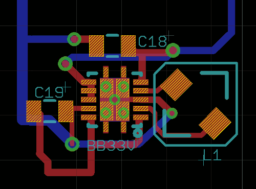
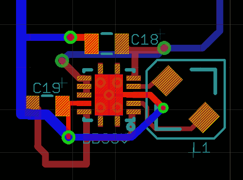
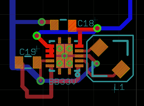
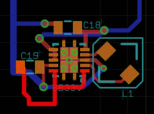
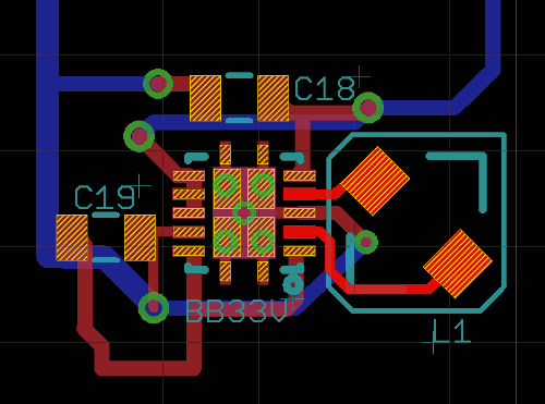
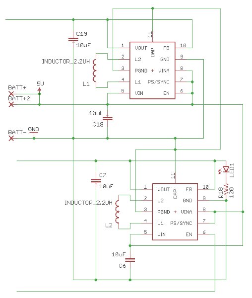
It's part of a more complex board, but I have currently only populated the TPS63001 and it's associated inductor and two capacitors, as per the example diagram on page 1 of the datasheet.  Orientation is definitely correct (made that mistake with a previous population), brand-new chip straight out of the pack.

  • There is something wrong with your circuit.  I would check the layout drawings and make sure the correct pins are attached to the correct nodes in the circuit.  As well, make sure the EN pin is taken high.  Finally, remove any electronic loads as these can pull the output negative.  Finally, you might order the EVM and test with that known good circuit and layout.

  • As far as I can see everything is as per the datasheet, see attached layout.  EN is attached directly to the li-ion positive, as per the Figure 1 of the datasheet.

    I'm testing the board purely with the buck/boost components populated, there are no other loads; do I perhaps NEED a load?  Testing output with a simple digital multimeter, can this have a "negative" impact?  This is my first design with a buck/boost.  Testing at battery (-) and Vout

    I'm trying to test whether my power supply design works before continuing to populate the rest of the circuit, no point buying the EVM as I would expect that to work as advertised.

    Board layout (stripped back) - note 180degree rotation

    ground traces highlighted

    source (Vin) traces highlighted

    output (Vout) traces highlighted (connects to pads further along on actual PCB)

    inductor traces highlighted

  • Thanks for sending your layout.  It will likely need to be better to get any switching power supply to work well.  Changes to make include: connecting all the GND nodes together at the IC, without traces and vias--these include the GND pins of Cin/Cout and the GND pins of the device.  Just tie everything directly to the thermal pad for a single point ground.  As well, the Vout trace to Cout needs to be much shorter--move Cout directly below the IC.  Finally, all traces that carry high current (Vin, Vout, GND, L1, L2) need to be thicker.  Since they carry high current, there will be IR drop.  You can look at the EVM for a good layout.

    I would expect your design would still turn on but not operate well.  To debug why it does not work at all, you will need to look at each pin's voltage with a scope.  Compare the signal that you see to what should be there.  Measure each pin of the IC with respect to its GND (local ground near the IC, not a ground point somewhere else on the PCB).

  • If that's the case with the grounds, why does the datasheet specifically separate out the control/logic and power grounds?  eg. it states that the PowerPad should be connected to PGND, and the description of the GND pin indicates that it is an entirely separate ground system from the Power ground; this indicates to me that they are to be treated as separate entities and not tied together, as is the case with many audio systems.

    Seems one has to be an electrical engineer to be able to use any of your ICs; following the datasheet won't result in a working system!

  • It is not uncommon to have separate grounds for the switching power returns and the quiet control signals that are electrically common at a single point.  The single point connection prevents circulating currents.

    Although these devices are meant for general purposes, most users are in fact electrical engineers, and the datasheets are targeted towards them.  We try to make the documentation complete and easy to understand, but we expect most users will have a basic understanding of dc/dc converter operating principles.

  • OK, I've spent quite some time on research, copying designs from EVMs etc., does this now look like it will work?  Cin and Cout have been moved as close as possible as per EVM, thick ground and source trace, inductor traces made more symetrical, etc.

    I've got a permanently enabled 63001 (bottom) for 3.3V general operation, and a 63002 (top) with MCU enabling for 5V supply (LED indicator when enabled).  Intending running directly of a li-ion cell.

    Are there further considerations when running two buck/boosts together like this?  And/or any considerations when testing just with a multimeter, eg. does it need a certain load to begin operating?

    Board layout (stripped back)

    ground traces highlighted

    source (Vin) traces highlighted; note 63001 is permanently enabled

    output (Vout) traces highlighted (connects to pads further along on actual PCB)

    inductor traces highlighted

    Any help greatly appreciated, as I think everything else is ready to get sent off for a prototype run (10 boards), but my power supplies have been incorrect on the past few runs so the boards have been wasted

  • I don't normally support TPS63001, but if you post your schematic, I'll look at your layout.

  • Hi John, please find below a snap of the stripped-back schematic, plus attached Eagle schematic and board layout if that makes things easier.

    Disregard the "5V" at the battery positive connectors, it's actually a li-ion so 4.2V max, down to about 3.0V minimum.  Top buck/boost is the 3.3V permanently enabled TPS63001, the bottom one is the MCU-enabled 5V TPS63002 with LED indicator.

    As far as I can tell I've laid it out as per the EVM and recommendations, but as I failed with my last layout I'd appreciate a checkover by those in the know - THANKS!

    1300.TPS63001_test.sch

    7002.TPS63001_test.brd

  • The layout looks ok. You could use wider traces for the inductor connections.


    Due to DC bias effects in ceramic capacitors (capacitance goes lower when they are operated at DC voltages higher than 0V) using only one 10uF capacitor on the output may not be enough. It is recommended to have at least 10uF capacitance. Please check the capacitor datasheet for the real remaining capacitance at the operating voltage you are using it.