This thread has been locked.

If you have a related question, please click the "Ask a related question" button in the top right corner. The newly created question will be automatically linked to this question.

LM5088-2 Vout drooping at medium/high load

Hello all,

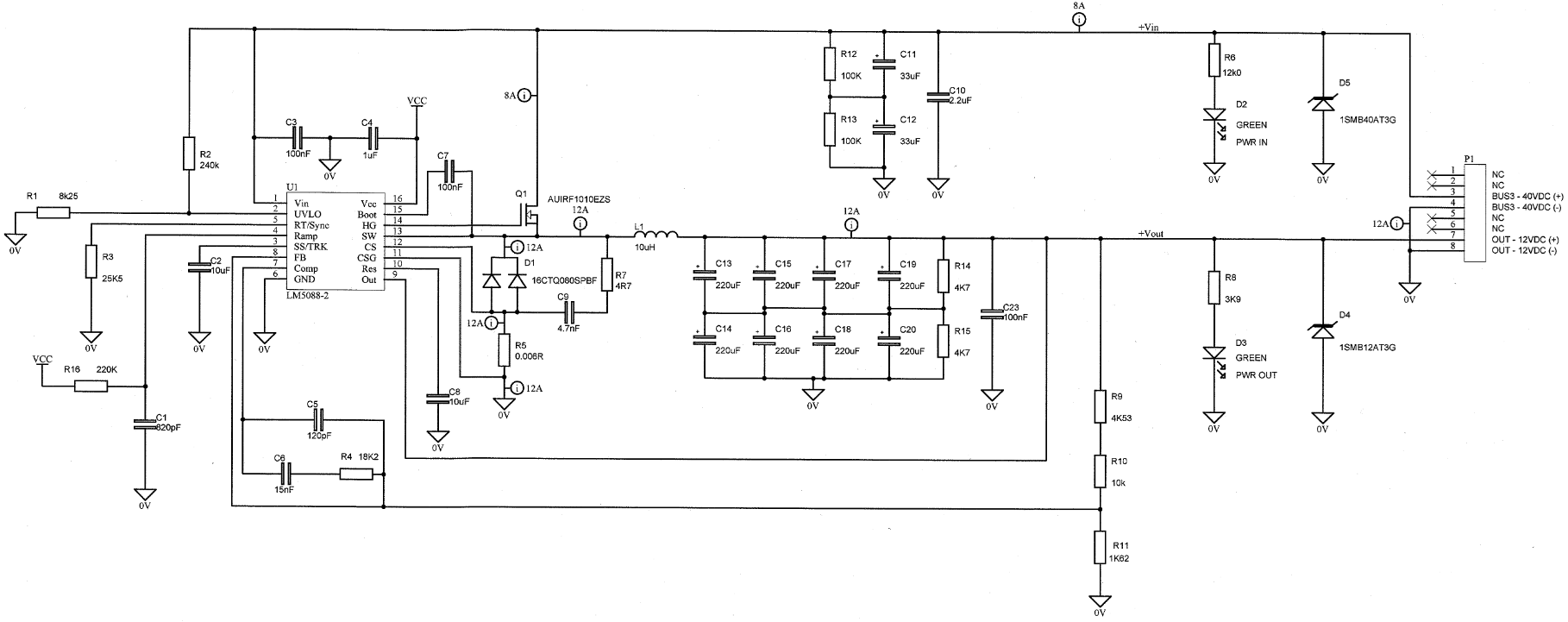
Please see the attached schematic.

The circuit is designed to run at a MAXIMUM of 10A at 12V (with 5% margin allowed).

The design criteria is 40VDC input and an UVLO limit of 36V (ish!).

I had some issues maintaining a stable 12V on the output at open load (the system requires that the 12V is stable even with no load) which was resolved with the addition of Rramp.

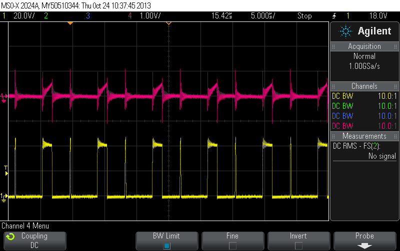
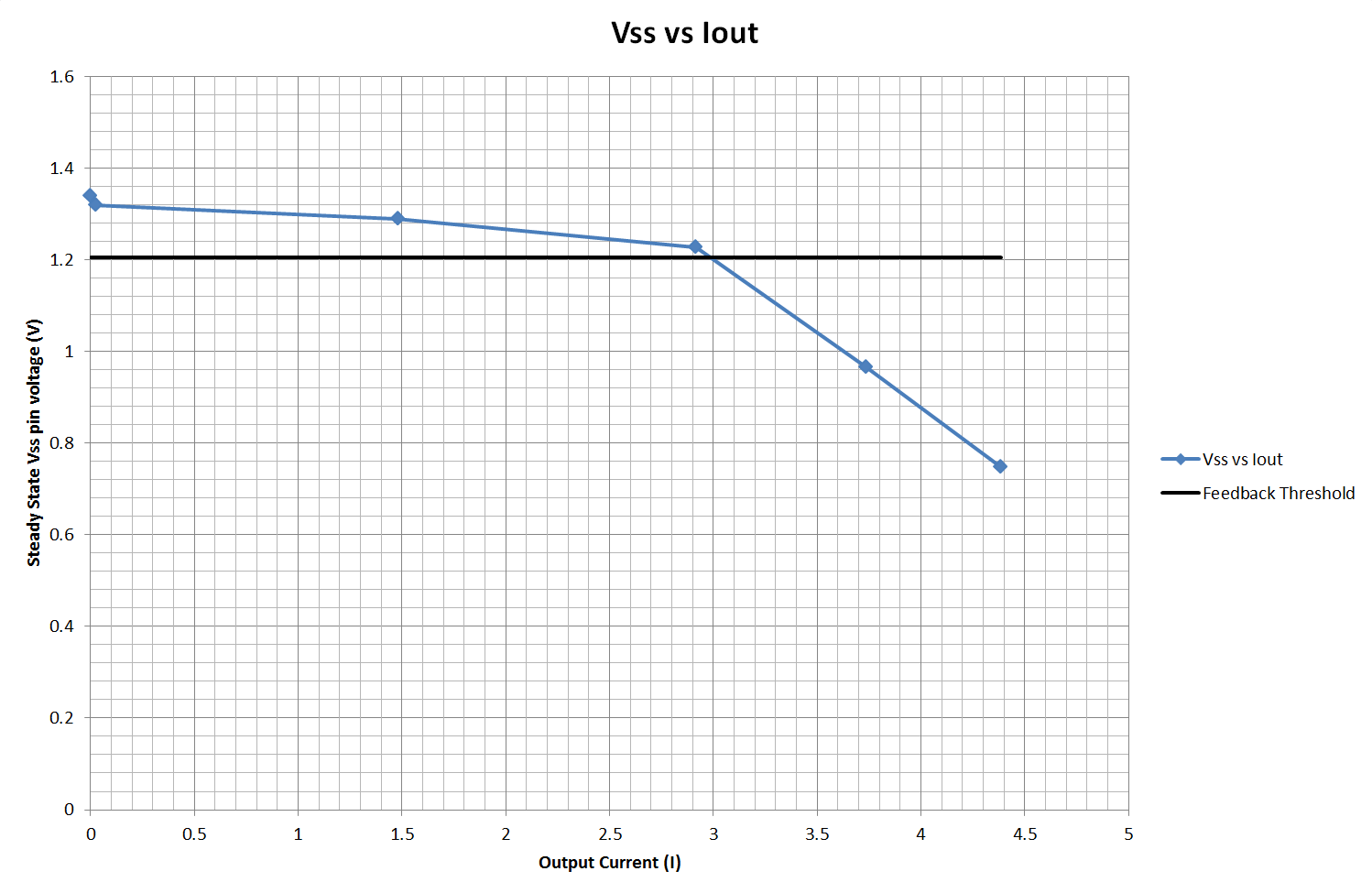
The electrical test we carry out runs the circuit at roughly 5A and the test is a pass if the voltage is within 5% of 12V. The result I have in the lab is that the output voltage drops to around 7.5V when a ~4.6A load is being driven. As shown in the attached scope trace the output itself is quite stable, my initial suspicion was that the ripple was quite high but that doesnt seem to be the case (the ringing shown is down to less than ideal scope probe placement).

I have re-run the calculations again just to be sure and the only discrepancies I have seen are that Chb (bootstrap capacitor) is a bit low, increasing it to 1uF has no effect. Also increasing Cvcc had no effect on the output.

I have attached the SW node waveform for reference. It looks to me as if the behaviour mentioned in the datasheet at the top of page 12 is being shown suggesting my ramp requires some more compensation, I reduced Rramp to roughly 115K and the output did not seem to change at all.

Any help would be much appreciated.

P.S: Qg for the mosfet is 56nF average, 86nF maximum. Peak inductor ripple current I have set to 40% of maximum in my calculations (4A).

Other parameters: Tss = ~1s, Trestart = ~240ms

  • Hi

    I thought it might be a current limit, but ther epsitmghiccup. Would you please capture RES pin wafeform ?

    Regards,


  • Hi Eric,

    Please see below the attached scope trace of RES pin (blue) vs SW pin (yellow), and also I have taken a scope trace of the RAMP pin (pink) again vs SW pin (yellow).

    Thanks for your input on this issue.

  • Hi Ian

    Does the output voltage drop gradually from 12V to 7.5V by increasing the output current ? or drops dramatically when the output current reaches 4.5A ? If the issue is caused by a curent limit, it will drop dramatically at 4.5A

    Please measure the COMP-GND(pin#7 to #6), FB-GND(pin#8 to #6) pin voltages and the R11 voltage using DVM when the output is 12V and 7.5V.

    Regards,

  • Hi Eric,

    The output voltage drops gradually as the load current is increased. I will take some measurements of the steady state output voltage at several different load currents and post the voltage vs load graph here when I am done.

    I will also get some scope traces of the COMP-GND and FB-GND.

    One thing I did notice (which I will also post later today) is that the soft start pin (SS) never reaches its theoretical clamped level of ~1.3V, I have already tested using a smaller Css of 1uF and it made no difference to the behaviour, the softstart pin seems to rise much slower than expected, around 1.5 seconds.......even with Css of 1uF which should theoretically have a soft start time of around 0.1s. The pin never reaches much higher than 750mV which seems to explain why Vout is lower than designed.

    I will add the steady state votlage of the SS pin also to my graph. Hopefully I will have these plots later today for you to look at.

    Cheers,

  • Hi. !

    if load transient response is slow you have to increase the crossover frequency . i.e. if load current has fast step from 0A to 5A and output voltage drops from 12V to7.5V and returns back to 12V then you have to increase the crossover frequency.  In first sight the crossover frequency of your design is less than calculated by webench tool.

    if Output voltage remain permanent 7.5V@5A then there may be some problem with current limit.

    I am writing this without analyzing your design in details 

    Regards

    Bishnu

  • Hi Eric / Bishnu.

    I haven't tested the transient response yet, the testing I am doing is from turn on of the input voltage.

    Please see the following images I have attached regarding both your answers today, they are the following:

    • COMP pin measurment at 0A
    • FB pin measurment at 0A
    • R11 measurment at 0A
    • COMP pin measurment at ~4.5A
    • FB pin measurment at ~4.5A
    • R11 measurment at ~4.5A

    Also I have attached the following:

    • Plot of Vout against Iout (A few loads just to see a pattern, I am using light bulbs as a load)
    • Plot of Vss against Iout.

    looking at the two graphs I have attached it seems the voltage drop I am seeing is infact related to the current output, not just a constant loss as I suspected previously (apologies!).

    I am still unsure as to what is the situation but maybe my layout is not ideal???

    Hopefully this information will highlight something I have missed.

  •  

    Hi Ian

    I guess it is caused by a noise injection.

    Here is something you can try;

    - Move snubber connection from the positive node of R5 to the negative node of R5

    - Kelvin-connect CS-CSG to R5 using twisted wire

    - Place a high quality ceramic capacitor directly from the drain of Q1 to the negative node of R5.

    Regards,