Hi
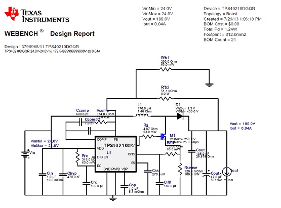
I try to use TPS40210 for our boost power supply design. I got a boost converter designed using Webench w/ device TPS40210 for 24V to 180V @ 0.04A boost converter. The schematic is attached. The only thing we changed from the schematic is we using 0.1uF/250V on Cout instead of 105uF.
The output voltage is not boosted to DC180V but DC23.5V (input - diode drop). On checking the frequency at RC (pin 1) is found to be about 330Khz and Voltage at BP (pin 9) is 8.14 V but no voltage at GDRV (pin 8).
1. Can the change of Cout cause this?
2. I use 24V DC switching power supply as the Vin, will it cause this?
3. When I make the GDVR open, it reads 7.85Volts. Otherwise it keeps 0V even I varied the resistant Rg from 4.87Ohm to 200Ohms, 2K and even 220Kohms.
4. I connected all the Ground point together with the Power Pad, will it cause this?
5. Do you have any evaluation board on this output range I can place order?
I appreciate with your help.
Regards,
Qing