This thread has been locked.

If you have a related question, please click the "Ask a related question" button in the top right corner. The newly created question will be automatically linked to this question.

LM3150 excessive output ripple

Other Parts Discussed in Thread: LM3150

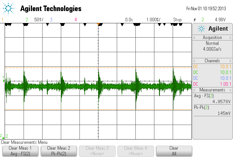
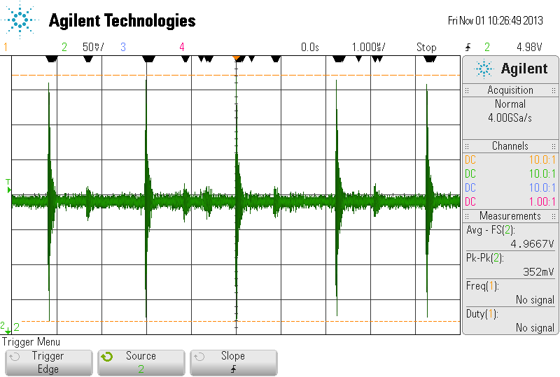
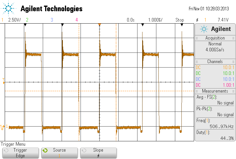
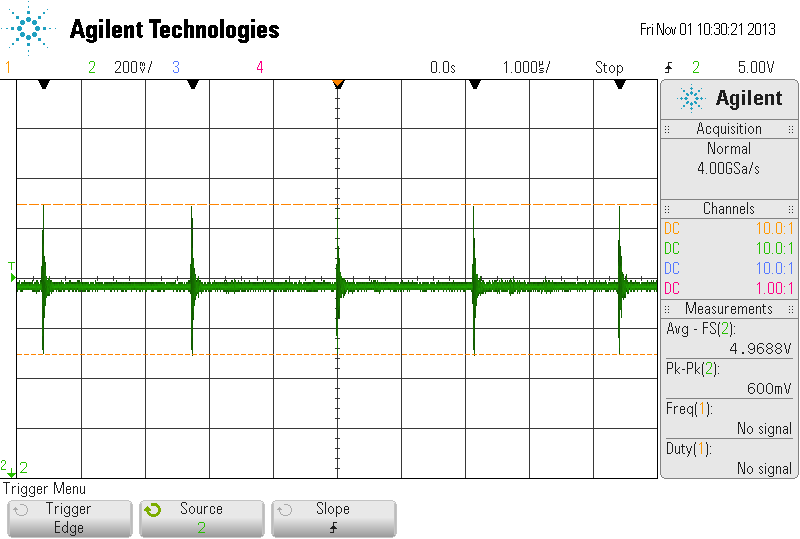
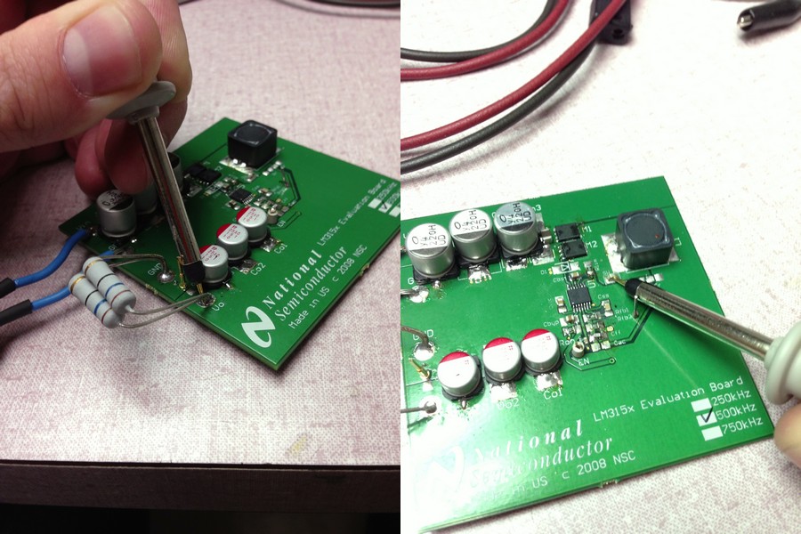
I am having issues with excessive output ripple using the LM3150 eval board.  The design goal is a 5V 1A output with 2.5A transient capability and 8V-32V input.  I have replaced several components on the board.  The input caps are 3x220uF 50V electolytics and a 10uF 50V X5R ceramic.  The output caps are 3x150uF 10V electrolytic polymers.  Both FET's are TI CSD18504.  Ron is 112K, RFB1 is 4.99K, RFB2 is 73.2K, and the inductor was replaced with a 47uH 1280 3A part.

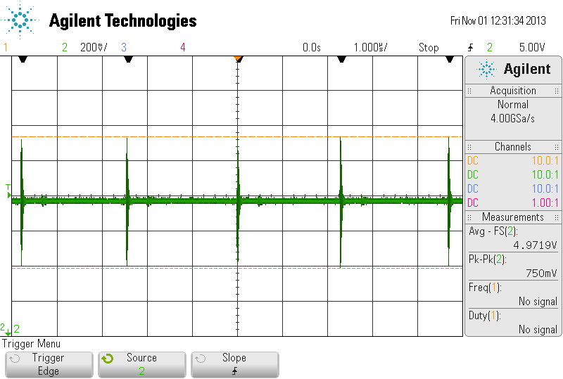
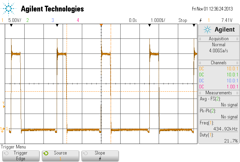
I have begun some basic load testing around 0.6A with load resistors.  The output ripple is a manageable 120mV below a 10V input voltage.  The ripple starts increasing above 10V, topping out at 750mV with a 18V input.  The ripple stays around 750mV as input voltage increases.

Any idea what's going on here?

EDIT:  I incorrectly listed a few of my component values.  RFB2 is 36.5K abd RON is 102K.

  • Can we see some waveforms?  Include the switching node and Vout.

  • When I tried to probe the switch node and Vout at the same time, the output ripple shot up dramatically, so I measured them separately.

    Output - 8V in

    Switch node - 8V in

    Output - 12V in

    Switch node - 12V in

    Output - 18V in

    Switch node - 18V in

    Thanks for any help you can offer.

  • What you are observing is "switching noise" not ripple.  As you have found you have to be careful when measuring this.  You will beet to probe directly across your output capacitors to measure this accurately.  Use as short a ground lead as possible, <1cm.  "tip and ring" method works well.  It looks like you may have quite a bit of overshoot and ringing on your SW node.  It may be due to poor PCB layout.  You need to keep the circulating loop from SW to Lout to Cout back to ground as small as possible with appropriate trace geometry.  You also neet to minimize the input circulating path by placing the input bypass capacitor as close as possible to the VIn and GND pins of teh device.  You may find it necessary to inculde an RC snubber fro SW to GND.

  • My variable supply is tied up with another test right now, so I used a 24V input.  I am using the LM3150 Eval board and the output capacitor current loop is rather large.  I could try moving them closer to the inductor.  I did move to a "tip and ring" measurement for these captures (see picture below) and the switching noise/ripple did not improve.

  • I measured the ripple across a 1uF ceramic cap placed after the output caps as recommended in AN-1900.  I measured a much more manageable 150mV of ripple.  I think all of my issues compounded from my measurement method and that there is in fact no issue with ripple on the output.  Thanks for your help John! 

  • I looked at the EVM users guide.  It appears that it is built so that a lot of different options can be supported, rather than trying to optimize using the ninimum number of compents.  You may not be able to get optimum noise performance from that layout.  I would suggest you try an RC snubber from SW to GND.

  • I happened to notice this post regarding supply noise measurments.

    FYI, I did some work with EDN to document the noise measurements you are talking about, along with a video.

    http://www.edn.com/design/power-management/4411821/Testing-a-power-supply---Noise--Part-2--

    Regards, Bob