This thread has been locked.

If you have a related question, please click the "Ask a related question" button in the top right corner. The newly created question will be automatically linked to this question.

TPS62090 fails with SW to GND short

Other Parts Discussed in Thread: TPS62090

Hi,

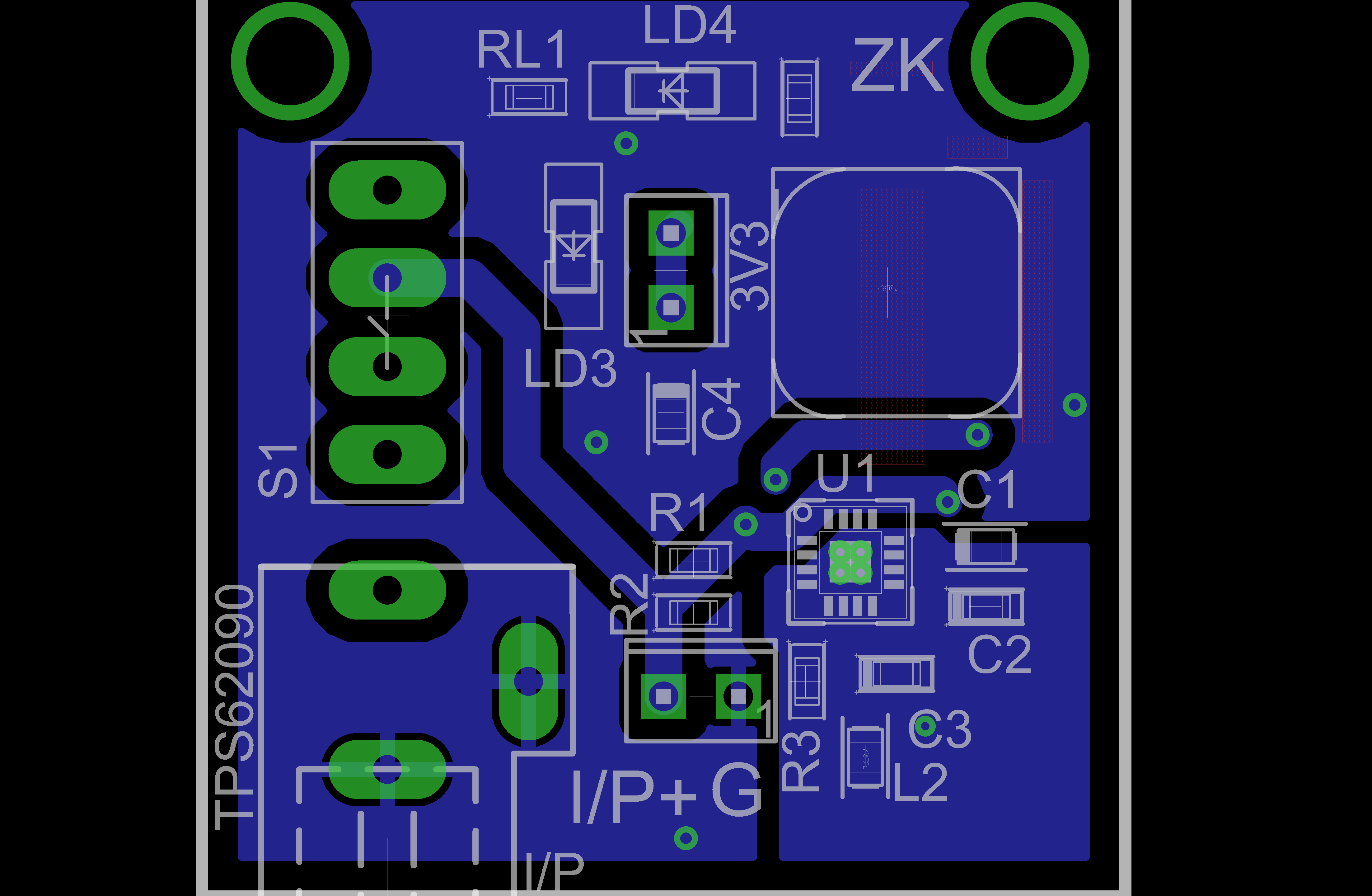
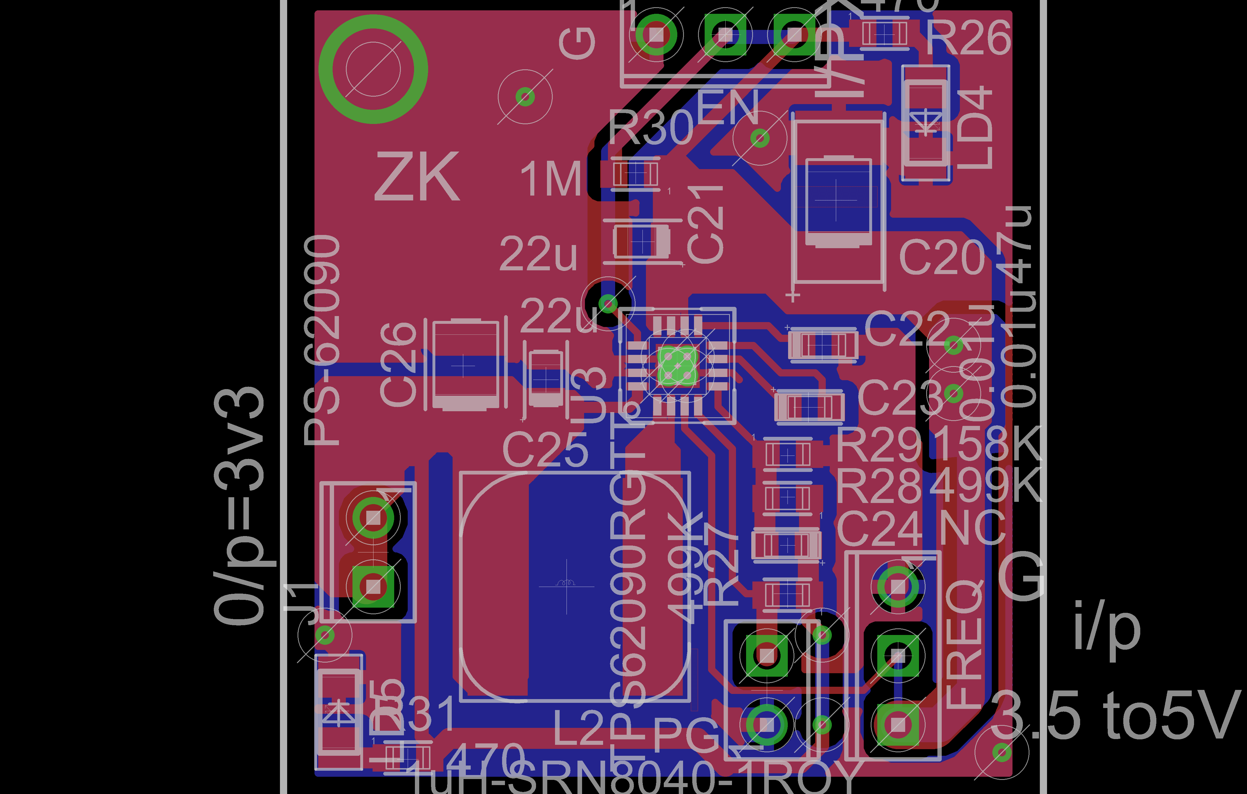
 We are using TPS62090 regulator(chosen by using web-bench) for our device(which consumes approximately 1A,input voltage for regulator is 5V dc). Initially all the things are working fine, but after few days (sometimes it will be in hours) the regulator will gets spoiled/ will give troble. Means the Vout(SW) and GND pin gets shorted and we getting 0V in SW pin. We replaced regulator so many times but we getting same issue.

Please check the layout diagram and provide your best advice to solve this problem.

Regards,

Naveen K  

  • Hello Naveen,

    Please provide the screen shots of the layout larger/higher resolution with the top and bottom layers isolated so that I can see them both clearly. On the order of two to three times larger would be nice.

    Also provide a screen shot of your schematic so I can follow through the nets to the layout.

    What is your soldering process? Do you clean the solder flux off of the border between the soldering and testing? This flux can have a habit of re flowing and providing conduction paths that can reek havoc on your system.

    Ryan May

  • Hello Ryan May,

    Thanks for your support. Please find image contains all view of layout and schematic.

    We are using manual soldering by hand using hot blower(smd rework station).We will clean the flux using isopropyl alcohol with a brush. This is for our prototype. All the things are working fine except power supply part. Please advice to solve the power supply issue. So that we can go for production stage. Our device consumes ~1A to 1.2A at 3.3V using 3.7V Li-Polymer battery.

    We will appreciate your earliest reply.

    Regards,

    Naveen K

  • It is clear that this layout does not follow the example one in the D/S (used on the EVM) very well.  Specifically, the SW node should not be routed through vias, the grounds should be tied together, not separated by an inductor, and the input cap should route very direct to the IC's pins.

    I recommend ordering the EVM and testing that known good design.  Then, copy the EVM design onto your PCB.

  • Dear Chris Glaser,

    Thanks for your suggestion. If we order EVM it will take some time,we need to re design and give it for fabrication at the earliest. So please advice to achieve design issue without EVM kit.

    Regards,

    Naveen K

  • If you want a reliable design, I strongly recommend prototyping before going to production.

    I gave my advice in the previous reply: copy the EVM layout onto your design.

  • Hi,

    We are facing  problems regarding to TPS62090 converter.We had spoiled so many regulators(GNDand o/p pin gets shorted) which has posted in the previous post "http://e2e.ti.com/support/power_management/non-isolated_dcdc/f/196/p/300653/1054219.aspx#1054219" . I have referred TI evaluation layout design for our new design which is shown below. So please check and verify the design and suggest me. Pls Let me know any changes required for our new design. So that we can give it for PCB manufacturer.

    Regards,

    Naveen K

  • Yes, this layout looks much better.

    I noticed that on your EN and FREQ jumpers, two of the pins are shorted.  This is likely not desired.

    A final improvement to the layout would be routing the grounds of C22 and R29 (that whole GND island) back to the AGND pin directly and not using a via into the GND plane.

  • Thanks for your advice.

    I kept EN pin high to enable the device, we don't know what is the advantages of EN and why should we disable the device?. Please advice about this.

    Regarding to FREQ please advice in what basis we can select the frequency and its advantages? 

    Regarding to ground of C22 and R29, in EVM design they shorted AGND(pin 6 and tab) and PGND(14 and 15) then connected to other ground pins using via. I have modified the design as per your advice pls check and advice which one is better. We thought, if we do like this we will mix the AGND and PGND and if we consider other things its difficult to connect C22 GND to PGND without using via  . So this is my confusion please clarify this.

    If any issues pls let me know we can modify as per your suggestion.So that we can save Ic's as well as money and time. 

    Regards,

    Naveen K

  • You would disable the device when that voltage is not needed by the system in order to save power.

    I guess my point was that those two jumpers are useless as the middle pin is hardwired to a voltage.  So, you can't use the jumper as such since putting the jumper across pins 2 and 3 would short Vin to GND while putting the jumper on the other end does nothing (those pins are already connected in the PCB).  So, it seems you might as well just remove the jumpers.

    The D/S explains about the tradeoffs of the FREQ pin.

    I think either of your layouts are ok.

  • Thank you very much for your advice.

    We will remove the connection between EN and Vin pin of the jumper if we use En to disable the device.

    Also advice if we use EN to disable the device we need to connect EN pin to any controllers right?

    Please advice how to control this pin that is if we connect EN pin to GND regulator output will be 0V or it produces sufficient(minimum) power to the system (like the system is in power saving mode because our system is like tab's so we don't want to turn off the system completely for saving data )? Its very important for our application to save power, because we are using Li-Ion Battery.So pls advice.

    D/S means datasheet right?

    Regards,

    Naveen K

  • Yes, D/S = datasheet.

    If EN is low, the device is completely off and outputting no voltage.  You should read the D/S of any device that you plan to use.

  • Thank you very much for your suggestions. This is my final clarification about DC to DC converter. Why most of the switching regulators are in QFN package in TI? why not in other packages like MSOP or SOT package?. Its easy to solder/handle right? If its no difference pls suggest 3A, 3.3V DC to DC regulator in SSOP/DGN package for our 3.7V(i/p voltage for regulator 3.2 to 4.2V ) Li-Polymer Battery applications.

    Can we use high voltage rated capacitors example: if the regulator enough for 16V rated capacitor can we use 25V rated capacitor instead of 16V.? Is there any issue like efficiency?

    Regards,

    Naveen K

  • Packages with leads are larger than packages without them.  The market desires smaller solutions, not easier to assemble by hand solutions.  The power quick search at power.ti.com can provide you a list of devices that are in a certain package.

    The voltage rating of a capacitor is not a variable in any efficiency equation that I know of.  Higher voltage ratings are fine, though typically larger.

  • Thanks for your advice. We appreciate your support.

    Regards,

    Naveen K