I have a design including the TPS40305 and CSD17313Q2 as both high and low side MOSFETs. The design is taken from WEBENCH (attached).
I have had problems with the high side NexFET beeing damaged (burning) several times on different boards during design test/validation.
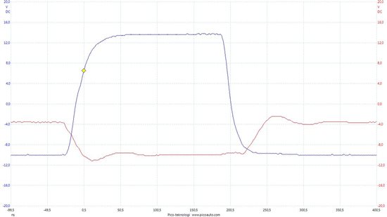
When measuring MOSFET gate voltages I see a quite large overlap during high side on, low side off which I think is the reason for the damaged MOSFET.
The VGS(th) of the CSD17313Q2 is normally 1.3V and seen from oscilloscope picture each switching thus causes a direct path from power to gnd during approximately 20ns.
Any suggestions?
Attached is an oscilloscope picture where low side beeing red line and high side beeing the blue. To be able to capture the complete curve I had to offset both curves -10V.
WEBENCH design:


