This thread has been locked.

If you have a related question, please click the "Ask a related question" button in the top right corner. The newly created question will be automatically linked to this question.

Regarding Vias located at input and output capacitor's GND shape...


Hi,

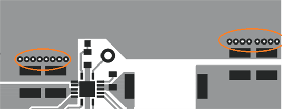
I am seeing in recommended layout of TPS54620EVM.

They have vias in row at the Cin and Cout Cap's GND terminals like this.

we also added vias, but they are not in order like this, random..

is this vias are to be in order?

or they can be any order....

  • The vias are intended to couple the ground at the input and output filter capacitors to the underlying ground plane.  The arrangement is not critical as long as they are close to the ground side of the capacitors.  In general an orderly layout tends to reduce unforeseen problems though.