This thread has been locked.

If you have a related question, please click the "Ask a related question" button in the top right corner. The newly created question will be automatically linked to this question.

TPS61202 failure when taking 3.7V to 5V

Other Parts Discussed in Thread: TPS61202

Hi-

I'm working with a prototype of mine that is using the TPS61202 to generate a 5V rail from a LiIon battery in order to charge a USB device at 500mA.  I have noticed occasional failures on multiple boards that I cannot yet explain.  The failure mode is that when I plug the load into the board, the 5V switcher draws ~1-2 amps until the chip smokes.

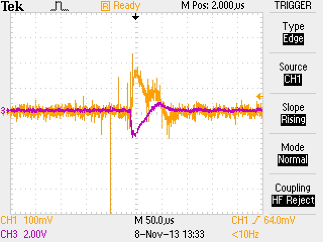
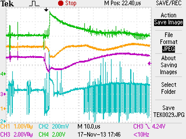
The circuit and layout are very similar to one listed in the datasheet, but I've attached them here to show what I'm doing.  In probing the inrush current, I notice that the target can take as much as 2A for 50uSec when operating correctly.  I am also attaching a scope shot that shows ch1 having 200mV across a 0.1 ohm series resistor to measure current, and ch3 showing the 2V dip that the supply does when the initial current spike occurs.  The response of the switcher looks well damped in this instance.  I have not been able to scope the system while a failure occurs due to the inconsistent failure rate.

Has anyone seen similar behavior?  Any ideas as to what might be the root cause?  Thank you!

  • Update: 

    I caught a scope trace of the 5V output when the chip failed:

  • You need to modifiy your layout to get the right performance,here are some suggestion:

    1 connect the positive node of C9 to Vout with wide and short trace.Your trace from R36 to C9 is too thin.

        I suggest move R36 to right and connect C9 directly to Vout with wide trace.

    2 Change the via on left top of C10 to the right side of C9.

    3 you can also route your Vin path with wide trace.So the Vin trace can completely cover the positive node of your inductor.

    4 I can not understand your input caps.C8 and C24 seems to be shorted?Why there is a trace between positve node and negative node of C24?


  • Hi Jim-

    Thank you for your prompt reply!  I'm getting some more parts later today to test with, and I'll deviate the design to accommodate some of the suggestions you listed (the ones that I can try without getting a new PCB. 

    The C8 and C24 input caps are difficult to see without the soldermask viewable -- the pads that you can see clearly is the positive pad of both caps.  The negative pads of both capacitors connect directly to the copper pour. 

    I took more data to get a better view of what is going on, and thought I would share it here.  Your response leads me to a couple more questions:

    1. Your suggestions, while valuable, seem to be small changes.  Would getting these few things wrong cause the chip to critically fail by frying itself?

    2. I would like to understand more about why this failure is occurring.  Would you be able to point me to any app notes, books, videos, or other resources that give a complete understanding of this scenario?

    Thank you again, and I look forward to your reply.

    2438.TPS61202 Failure Testing.pdf

  • Do you have waveforms on SW pin when you plug in the load.

    You have mention the chip smokes.So ,I suspect there's short between SW and ground.

    This is the most case happens on chip damage.

    Bad layout can cause high spike on SW pin ,which can make SW pin shorted to ground

  • Hi Jim-

    Thanks for your reply.  I'm not sure what you mean by the SW pin -- the datasheet doesn't mention a SW pin.  However I did take a couple scope shots of the system when I plugged in the load.  Both scope shots have the same probe connections:

    Ch. 1 (yellow) is on Vin, Ch. 2 (Blue) is on pin 3 labeled 'L', Ch. 3 (pink) is on Vout, and Ch. 4 (green) is on pin 1, 'Vaux'.

    The first scope shot, '13.11.17TEK0029.jpg', shows what the system looks like when it starts up fine.   The second scope shot, '13.11.17TEK0030.jpg', shows what the system looks like when it fails and smokes the chip. 

    Would this suggest that there could be a potential problem?  If so, what might that problem be?

    Thanks again!

  • Hi James:

       Thanks for catching the waveforms.

       SW pin is same as L pin in this case.

       Change 2 looks strange to me.For a boost converter the waveforms of this pin should be a pulse,the low level is 0V and the high level should be Vout voltage.Your vout is 5V,but the high level of your L pin is around 1V?Could you please check again?

        If you can catch the inductor current ,it will be much helpful.You can lift your inductor up and connect a wire between inductor pad in your pcb to positve node of your inductor and then use your current scope to catch the current going through the wire.

  • Jim-

    Thanks for your quick weekend reply.  As for Ch.2, I think you can assume that my probe/scope were not set with a matching '10x' setting.  If you multiply the scale by 10 the readings are what you would expect. Please consider that the scope's scale is off by a factor of 10.

    I'm afraid I have a TEK2024B scope without a current probe.  Is there anything that I can do to get this measurement without one?  Even if I can get the probe purchase approved, it will take time to identify and purchase a suitable current probe. 

    What are you thinking is going on?  Do you have any theories that would explain the chip killing itself?  The team is running other mechanical and firmware tests and occasionally need me to repair the boards.  I was hoping to find a fix that could be applied on these PCBs to keep the chips from breaking to streamline their prototype testing.

    Thank you!

  • Hi James:

        Thanks for clarifying the scope setup.

        After multiply the scale by 10 for CH2,the maximum voltage on this pin is 10V. This is too high for our boost,it can cause damage to the chip. You should keep SW voltage below 7V,and you can achieve this by modify your layout.

        Your could also contact your local FAE for help.

  • Hi Jim-

    Thanks for the insight and pointing out the out-of-spec operation of the 'L' pin.  In order to test the system with your layout suggestions, I made the change to my existing board as described below in text and with a drawing. I believe this solves all of the layout problems you brought up in previous comments, however I'm still seeing 8-10V on the 'L' pin of the part as shown in the scope shot below.  Do you consider the changes I made to be valid? Can you think of what may be causing this given the changes made?

    I'm looking for a solution that I can apply to these current boards so we can continue system testing while waiting for the next board rev to be designed and built (2-4 weeks).

    Board change description:

    1. Add a 10uF X7R capacitor directly at the output pin of the switcher
    2. Add a 22AWG wire from the +Vin trace to the two input capacitors and L2
    3. Cut the trace on the bottom side going from Vout to TPS61202 pin 10 and replaced it with a wire from a via further downstream from the output capacitors.

    Board change drawing:

    Scope trace after applying the board change.  Ch 1 is Vin, Ch 2 is on the 'L' pin, Ch. 3 is Vout, and Ch. 4 is not connected.  This is in 'idle' operation of the part with something like 30-50mA of load current.

    The following scope image has the same channel configuration, but show how the system performs when a heavy load is inserted and it reacts well (i.e. not smoking).  This suggests that the changes I made to the PCB to correct layout errors didn't offer any improvement as the 'L' pin nearly reaches 10V:

  • Hi Jim-

    Have you had a chance to see the new data I posted?  I think it suggests that the layout issues found may not be the complete solution.  Another chip failed this morning and I'm hoping to streamline the testing process with these boards.

    Thanks,

    James

  • James:

         Is your SW voltage finally go zero after the failure?If so ,there's a very big possibility that the failure is caused by layout.

  • James:

          Layout is something you can improve to make your system more robust.Also,I suggest you contact your local FAE for support.Because he can see your real board and system.