This thread has been locked.

If you have a related question, please click the "Ask a related question" button in the top right corner. The newly created question will be automatically linked to this question.

TPS54218 mininum load

Other Parts Discussed in Thread: TPS54218, TINA-TI

Dear Forum,

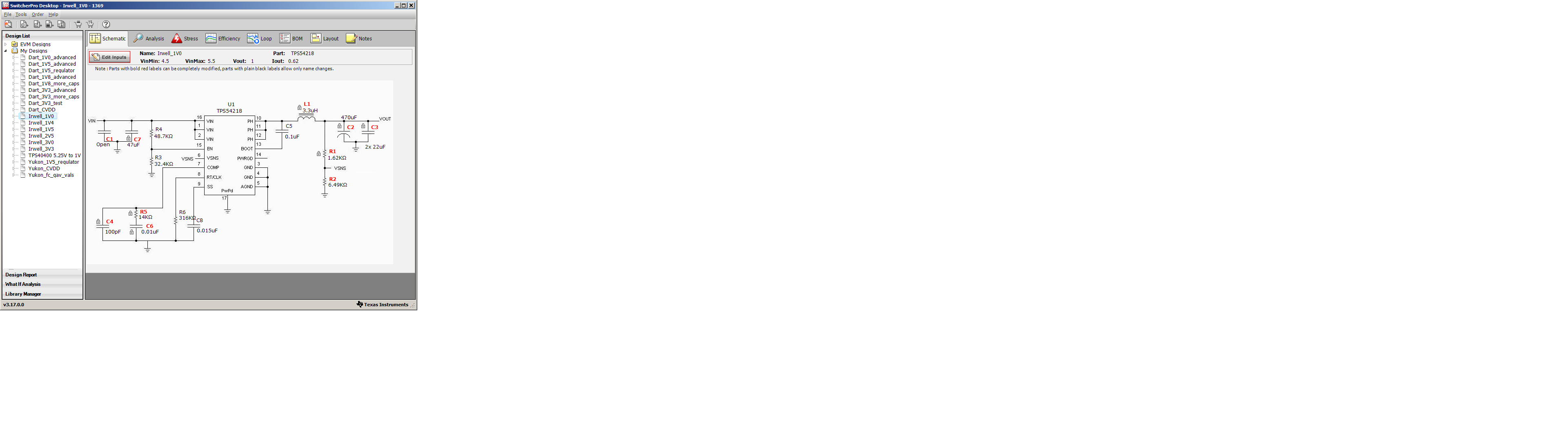
I wish to use the TPS54218 (2A step down switcher) to create a number of voltage rails within my design. However, the minimum load on some of these rails can fall pretty low (10mA) and I am concerned that my TPS54218 design may not work properly at these low loads.

The reason for my concern was that, in July 2013, the data sheet was updated to Rev B and a paragraph was added:

"COMP VOLTAGE LEVEL

....Proper application circuit design must ensure that the minimum load steady-state COMP voltage is above the +3 sigma minimum clamp to avoid unwanted inhibition of the high side power switch."

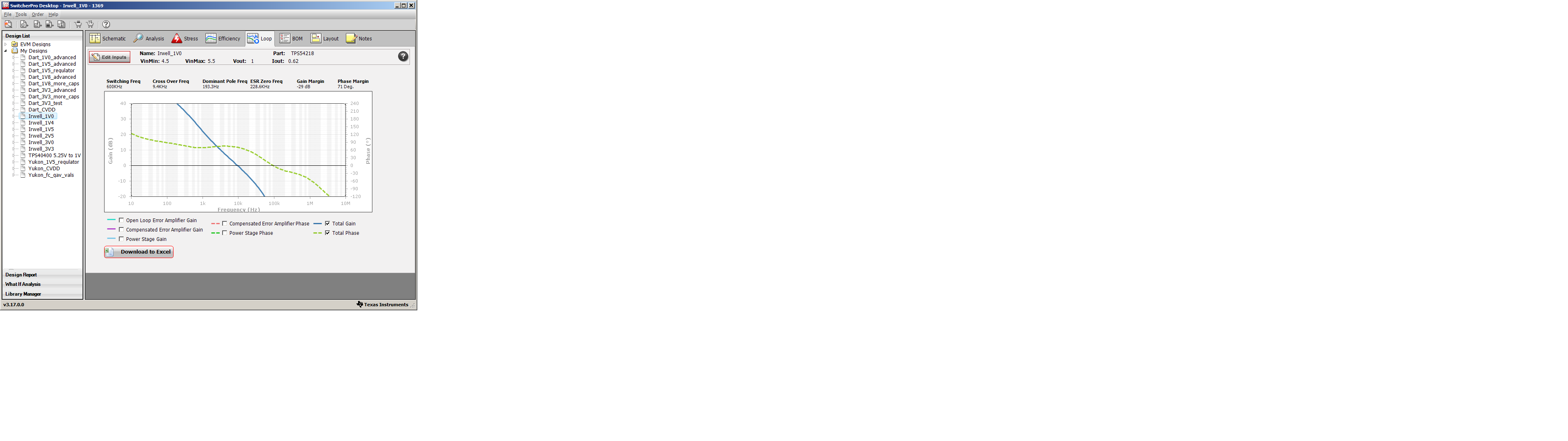
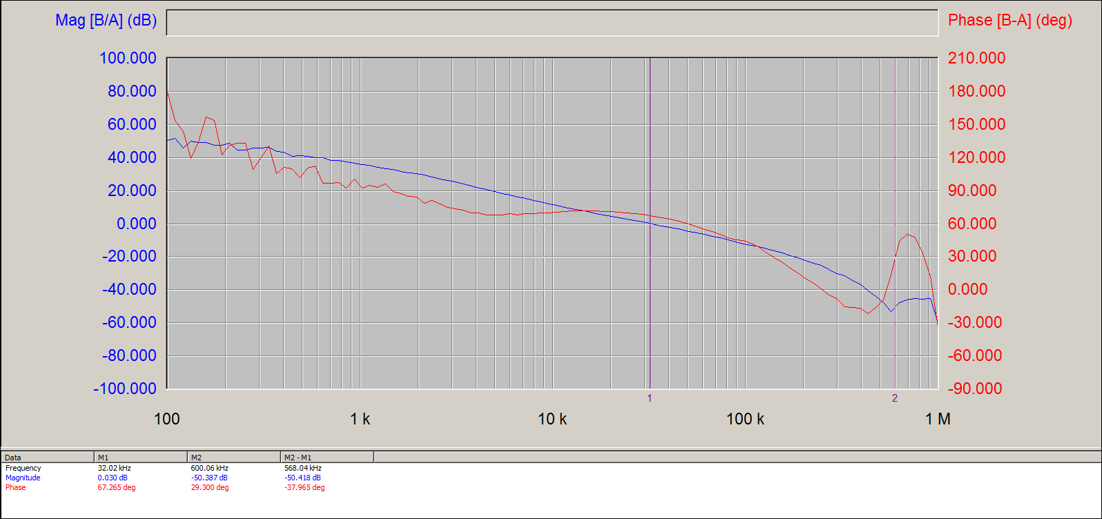
The good news is that datasheet Figures 48 and 49 imply that the regulator works down to zero load.

Is the solution to choose an inductor ripple current that is large enough for the peaks to exceed the required level even at zero load? If so, what is the peak current level that I need to achieve?

Thanks for your help.

Best regards,

Gavin.

  • Hi Gavin -

    The TPS54218 is fully capable of operation at zero load current.

    Being a peak current mode device, it's COMP level rises/falls as the peak inductor current rises/falls. TPS54218 has a "minimum" comp level, below which switching is inhibited.

    Generally, you should be OK as long as you follow the datasheet recommendation of sizing your inductor ripple for 20-40% of the device's full rated load of 2A. Some designers try to push the output ripple very low by using a large inductor, which makes the ripple current very small, and can in some cases push the no-load comp level near the minimum clamp. This is only really an issue at zero load, as any load current increases Comp to begin with.

    The Comp to Ipeak relationship is actually quite complicated to estimate, so the best bet would be to run a quick transient spice simulation of your design to look at the Comp level. We have a Tina-TI (free spice program from TI) model of this which can be used for this purpose.

    This is just something you'll want to be aware of when evaluating your hardware. It can be easily handled by tweaking the inductor value or switching frequency.

  • Hi Matt,

    Thanks very much for your response. Based on this, I have used SwitcherPRO to implement a 5V to 1V converter using a 600kHz switching frequency and a 3.3uH inductor. This should give a nominal ripple current of 510mA. The schematic is shown below:

    At the maximum load current of 0.62A, the Bode plot looks good, as shown below:

    If I change the design parameters to reduce the output current, the Bode plot continues to look good down to 0.2A. However, below this, it starts to look bad. At 0.002A, SwitcherPRO displays an error message saying the design is unstable. The Bode plot at 0.01A is shown below:

    Is this design really going to be unstable at low currents, or is this a flaw in the SwitcherPRO model?

    I am trying to get a second opinion from TinaTI. I have found a TPS54218 Transient model in the library, but it has a pin DUMMY_TEMPIN that I don't know what to do with. Leaving it unconnected causes an error message when I run the simulation. What is this pin for?

    Best regards,

    Gavin.

  • One thing I noticed, you have mixed output capacitors at C2 and C3.  SP will let you input those, but does not actually support them in any calculations.  You will have to use only one type of capacitor to get any meaningful results.

  • Hi John,

    If I remove or change either C2 or C3 then the Bode plots output by SwitcherPRO change also. It therefore seems that both output capacitors are included in the Bode plot calculation. Are you saying that SwitcherPro ignores C3 when suggesting values for the compensation components?

    Please can you also comment on the validity of the Bode plot at low output current (as per my previous post)?

    Thanks,

    Gavin.

  • The Dummy Tempin pin isn't used. It is part of the model for compatibility purposes with other simulators. You can simply ground the Dummy Tempin pin. there is also a convenient Tina-TI Transient reference schematic which is set up properly already, so you can simply change your external components and "go".

    We also have the same type of reference schematic for the small-signal (averaged) model, which should provide more accurate results when using mixed output capacitor types (i.e. different capacitance/esr/esl)

  • What I mean is that the capacitors are not modeled correctly.  SP is using them in the calculations and loop plots, but the plots are not correct.  if you need to have mixed capacitors you will have to model that in pspice using the average model (that is what I personally use and recommend).

  • Thanks John. The pspice simulations are making a lot more sense than the SwitcherPRO plots. For one thing, the Bode plots produced in pspice show little variation with load current. Is this what you would expect?

    I now need to go back and re-optimise the compensation on all my regulators.

    I wish I had known that SwitcherPRO was broken before I did my last project too.

    Best regards,

    Gavin.

  • Switcherpro is not really broken...it's just that the mixed output capacitor feature was never fully implemented.  The capcitor placeholders were put in place, but the impedance model was not completed before development stopped for that tool.  It stillis a useful tool for some things, it can do a lot that webench (the tool that replaced it) cannot.  Work on switcherpro was completely stopped, so they did not go back to remove that half built feature.  Most of the users are familiar with these limitations and know how to work around them.

  • To help me understand what the potential issues are with my previous designs, optimised using SwitcherPro, please can you clarify the following:

    Why is it that the frequency response results from SwitcherPro change so dramatically when the load current is reduced (with all component values fixed) whereas pspice suggests the frequency response remains approximately constant across load current variation? This seems to be true even with designs having only a single output capacitor type.

    Thanks,

    Gavin.

  • I would really have to dig into that.  It had been a long while since I have used switcherpro much and while I know the TPS54218 well, it brlongs to another product line so I have not worked with it much in a couple years.  I often respond to forum posts outside my product line if I have something meaningful to contribute, but I can't really spend a lot of time on other parts that don't directly support.  I can take a quick look to see if there is something obvious.  For simple current mode model, the loop response does greatly depend on load current as if you ignore slope compensation,the filter pole frequency = 1 / ( 2 * pi * (vout/Iout) * Cout).  Maybe that is what is going on with this model.

  • Hi John,

    Having experimented some more, I am finding that, at larger output currents, the bode plots produced by SwitcherPro and PSPICE are roughly in agreement. However, when configured for small output currents, SwitcherPro often shows designs to be unstable whereas PSPICE shows they are fine. To illustrate this point, I used the TPS54218 EVM reference design, without modification, in both SwitcherPro and PSPICE. Note that this design uses only one type of output capacitor.

    For the default output current of 2A, the bode plots from both SwitcherPro and PSPICE are shown below:

    Both show a cross over frequency around 40 to 50kHz and a phase margin around 50 to 60 degrees. There is less agreement on the gain margin, but both show this to be at least 27dB.

    I then configured the output current to be 10mA. In PSPICE, I changed the load resistor from {1.8/2} ohms to {1.8/0.01} ohms. In SwithcerPro, I used the "Edit Inputs" button to change Iout Max from 2A to 0.01A. The resulting bode plots are shown below:

    Now the two methods give very different results. PSPICE shows the cross over frequency to still be around 50kHz (as expected based on Figure 32 in the datasheet SLVS974B), the phase margin is around 50 degrees and the gain margin is over 40dB. However, SwitcherPro shows the cross over frequency has fallen to 2.4kHz and the phase margin becomes dangerously small around 500Hz.

    If I configure the output current to be 7mA, SwitcherPro produces an error message stating that the phase margin is too low, whereas PSPICE shows the stability to be fine.

    In conclusion, what I would like to know is:

    Is the TPS54218 EVM definitely stable down to zero load? And, when configuring models for low output current, can I trust the output from PSPICE and ignore the output from SwitcherPro?

    Best regards,

    Gavin.

  • It's been a couple years since I have worked with TPS54218.  I would have to look at the power stage gain and phase characteristics to see what is going on with the two models.  If you have a TPS54218 EVM, you could always measure the loop to see if it agrees.  I doubt that I have an EVM available (I don't normally keep any boards for parts I don't support), but if I can find one I'll take a quick measurement as I a network analyzer on my bench today.

  • Here's a no-load bode total system bode plot of the TPS54218 EVM I have from a few months back. It shows about 60 degrees phase margin and about 10db gain margin. 

  • I took a quick look at SP.  The loop response stays consistent unit the device enters forced CCM operation.  I think the loop response is only valid so long as the set load current is greater than one half the peak to peak inductor current.

  • Hi Matt, John,

    Thanks for the responses. The plot posted by Matt roughly agrees with the PSPICE result.

    I'll ignore the SwitcherPro results for the low output current case and use the PSPICE results instead.

    Thanks again for your help.

    Best regards,

    Gavin.

  • Hi Matt,


    Further to our discussion back in December, I now have my boards assembled and running. The regulators seem to be working well, but I am worried about the COMP voltage level on one of the TPS54218 devices.

    The device in question implements a 5V0 (+/- 3%) to 1V0 regulator. I am using a 3u3 +/- 20% inductor and a switching frequency of 600kHz +/- 1%.

    During the system boot time (several seconds), the devices that use the 1V0 rail are held in reset and consume little current. In this state I measure the COMP pin voltage to be 564mV at 27 degrees C. This is a little below the +3 sigma minimum clamp voltage shown in the data sheet. Do I need to fix this?

    If the COMP voltage does fall below the minimum clamp level, what are the consequences of this? Will the output voltage fall out of regulation, or are the consequences more subtle?


    Thanks for your help.


    Best regards,

    Gavin.

  • Hi Gavin -

    The +3 sigma level is appx 590mV at 27C, so this design is fairly close. 

    The effect of reaching the minimum comp clamp would not necessarily be a loss of regulation, it would be increased output ripple. When the comp signal reaches the clamp, the TPS54218 will simply skip the next pulse. During this time, the control loop will bring the comp signal back up above the clamp. During the skipped pulse, the output voltage will dip because of the skipped high-side pulse, and when comp recovers, at the next switching cycle, the control loop will increase the duty cycle accordingly to maintain the output voltage its set point. Its possible that the comp signal could not be raised back above the clamp in a single cycle, in which case, there would be more ripple, because of 2 skipped pulses etc... Depending on your output band requirements, this could pose an issue. 

    To avoid such an issue, the output inductor value could be reduced, I would start with 1uH-2.2uH, or the switching frequency could be decreased. 

  • Hi Matt,

    Thanks for the response.

    As per your suggestion, I have now tried a range of inductors and the results are summarised below. The Iripple values are the nominal values calculated using Equation 19 in the data sheet. The Vcomp values are those measured on my board using a 1Mohm active 'scope probe. The ambient temperature was 25 degrees C.


    L              Iripple      Vcomp

    3.3uH     404mA     577mV

    2.2uH     606mA     585mV

    1.5uH     889mA     589mV

    1.0uH   1330mA     617mV

    It seems I need to increase the peak current a lot in order to get small increases in the Vcomp DC output level. Is it possible that the device I am using has a Vcomp output level (and presumably also a Vcomp clamp level) that is significantly below the nominal shown in the data sheet?

    I would prefer to avoid a large Iripple value so as to minimise output ripple and maximise efficiency (the maximum load current anticipated is only 620mA). I am therefore thinking of using the 1u5 inductor value, which just about achieves the +3 sigma Vcomp value on my sample set of one unit. Does this seem sensible to you?

    Best regards,

    Gavin.

  • Hi Gavin- I would probably recommend playing it safe. Though the chances are low if COMP is sitting close to the +3 sigma "tail," it's still possible that some small percentage of devices will have pulse-skipping at this condition. If efficiency is a concern, you could also decrease the switching frequency to increase the ripple current. This will actually increase efficiency in general due to reduced switching losses. 

    Minimum comp-based pulse skipping is not necessarily a loss of regulation, but it will cause larger Vout ripple when it occurs, possibly enough to start tripping the power good signals, etc... The condition will also disappear when load is applied, so I suspect it would be only for a short time in your end system as well. 

    If you contact me offline, I can share a waveform, which may help give a better idea.