This thread has been locked.

If you have a related question, please click the "Ask a related question" button in the top right corner. The newly created question will be automatically linked to this question.

LM3150 LAYOUT SUGGESTIONS

Other Parts Discussed in Thread: LM3150, LM22677

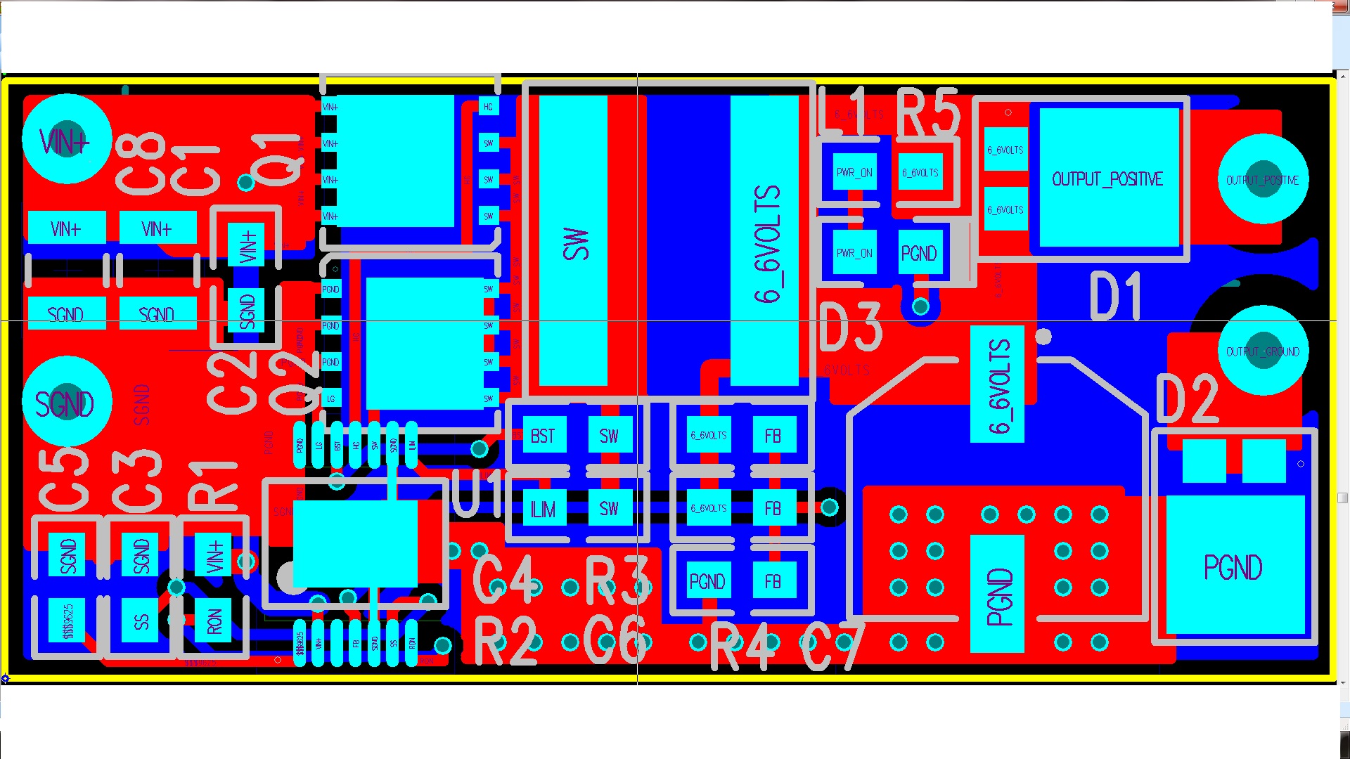
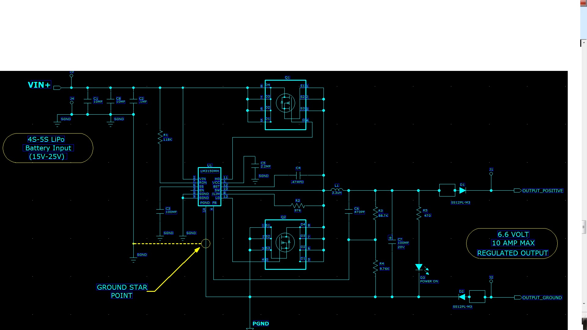
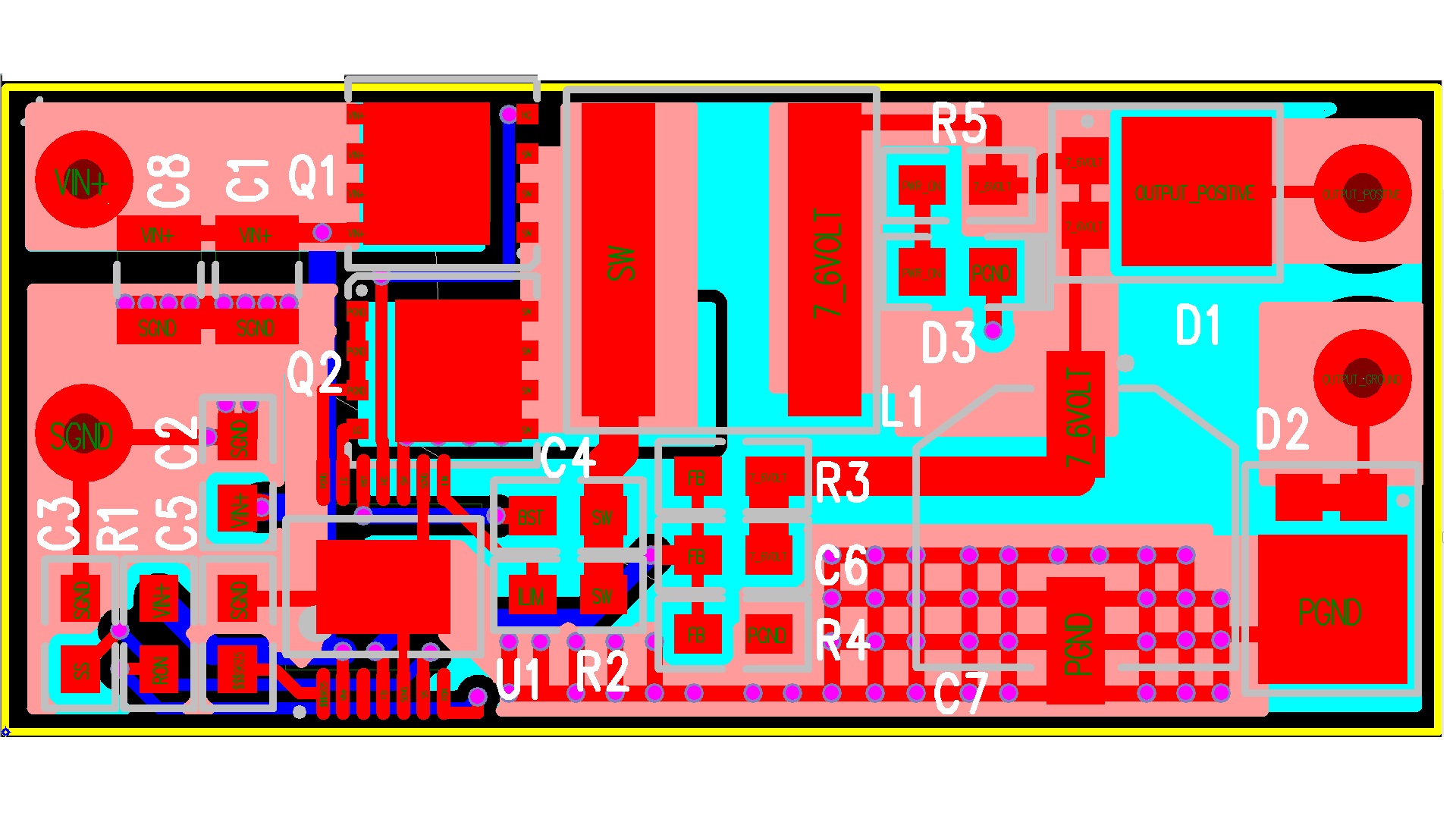
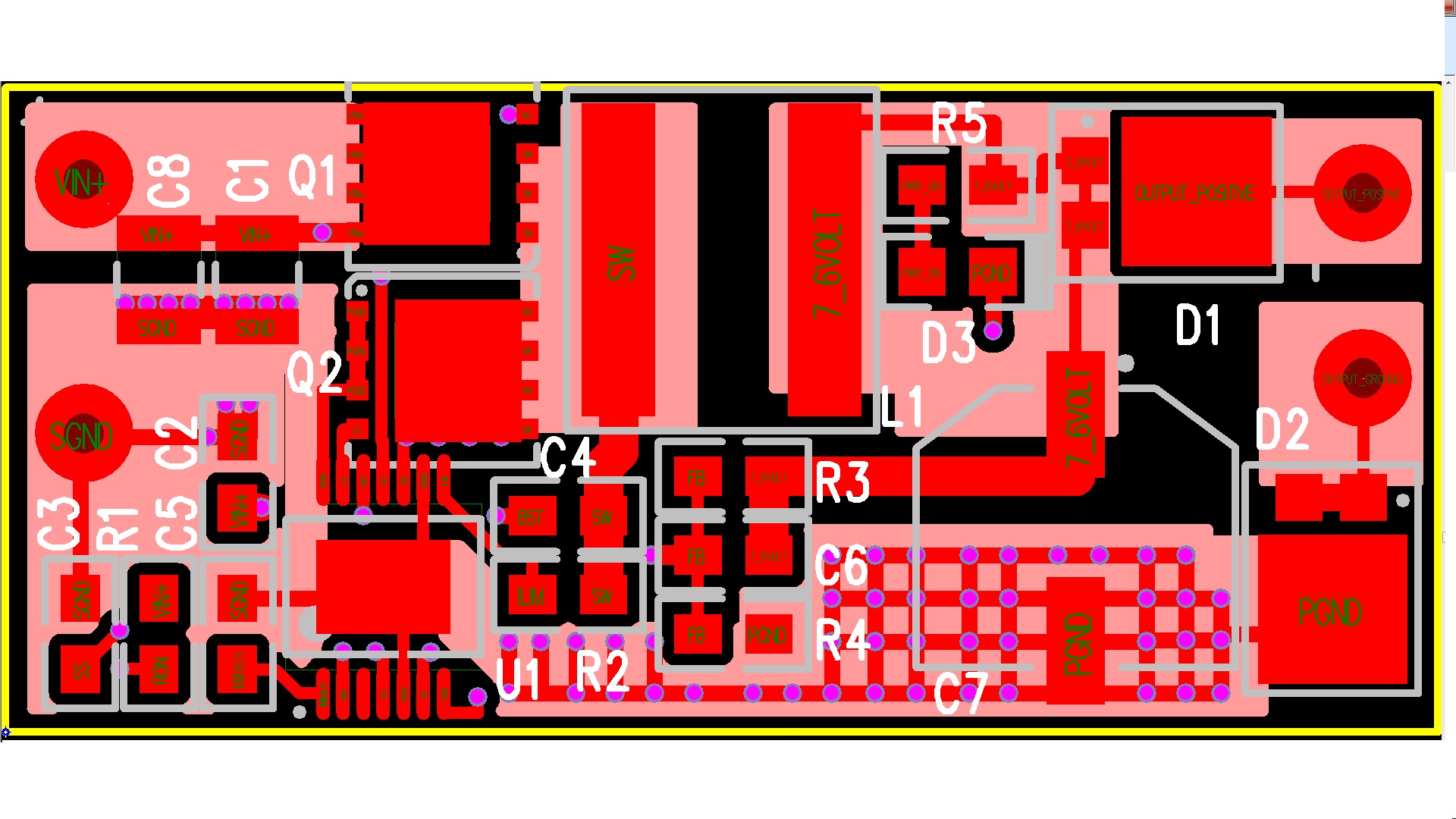
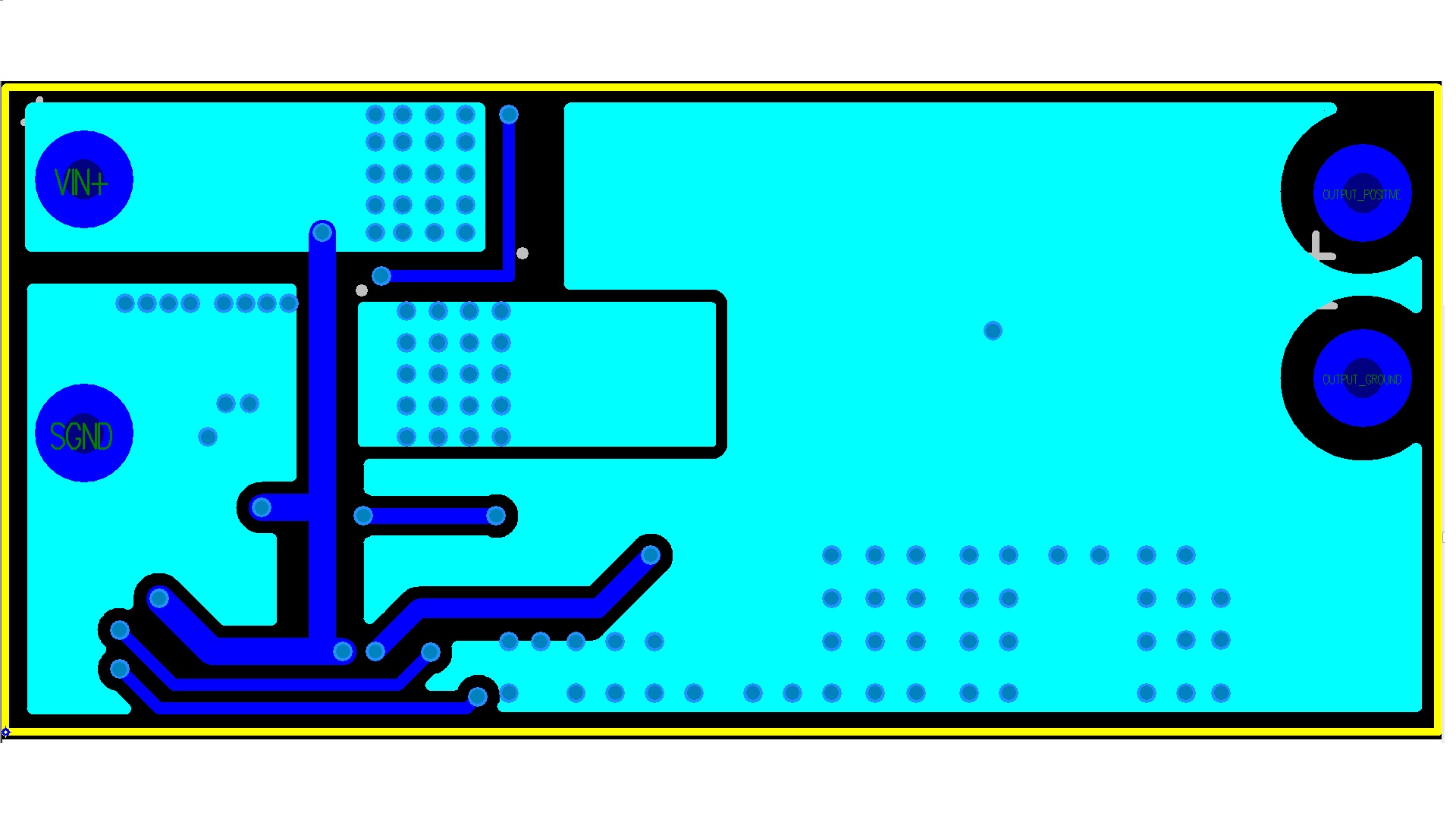
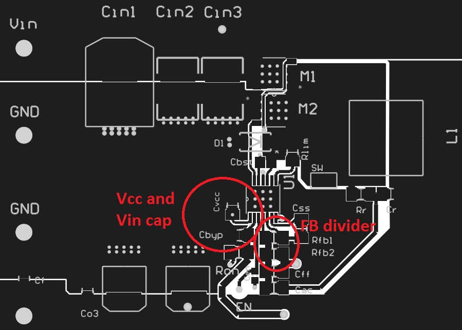
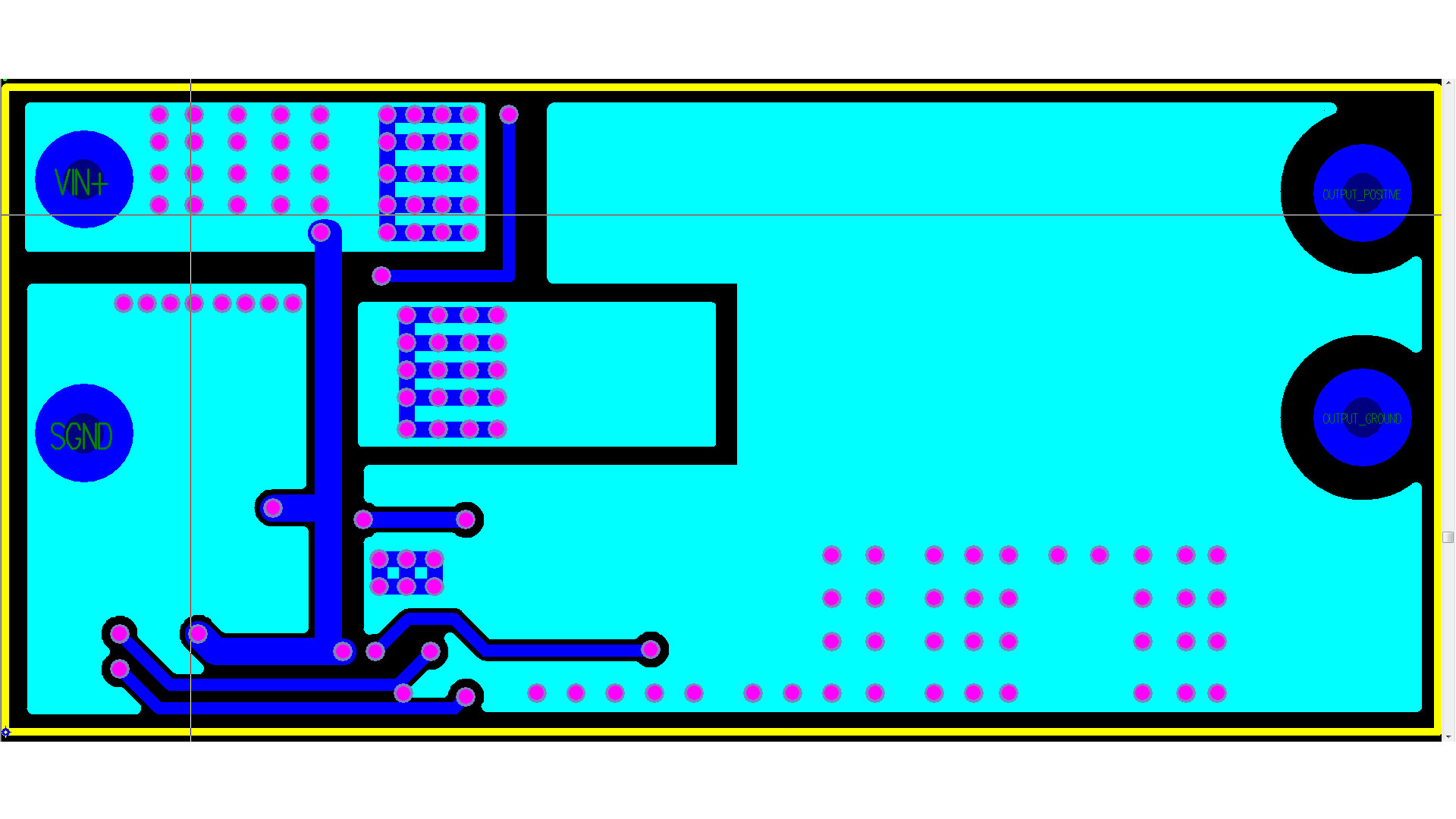
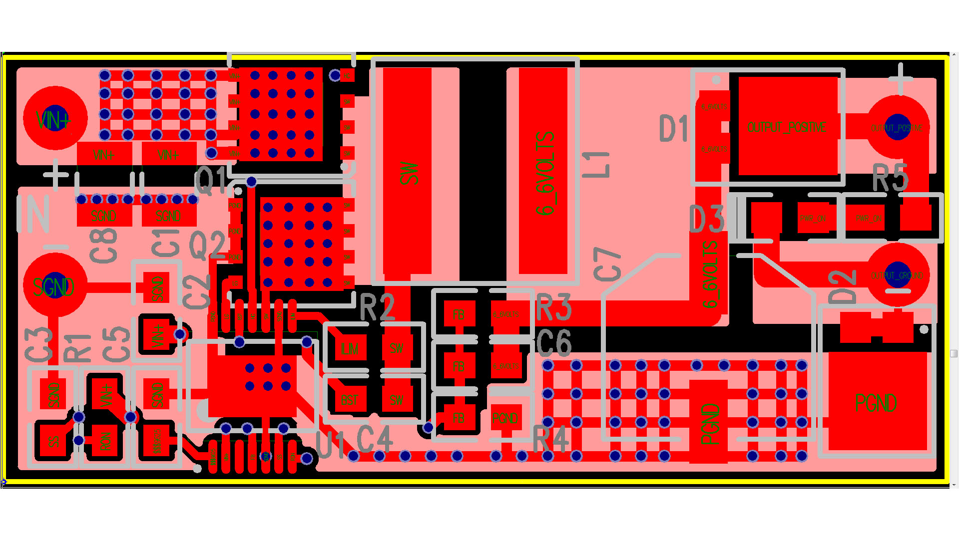
I just finished the layout of a buck regulator board and would like to see if I can avoid some problems by having a second set of eyes look over the design.

I have attached both the schematic and the board layout and would welcome any and all suggestion that would result in a stable and quiet design. You will note that the board is not a multi layer but simply a two sided design.

Thank you very much for your help!

Steve


  • Hi Steve, 

    Yes, we can review the layout. Thanks for doing this before sending it out.

    I did not see the attachments, could you attach the files one more time?

    Regards,
    Denislav 

  •  


    Denislav,

    Thank you very much for your QUICK reply! Here are the images.


    Have a great day!


    Steve

  • Hello Steve, 

    Here are some comments on the layout:

    0434.LM3150_LAYOUT_REVIEW.pdf

    Also, see the app note for the evaluation board: http://www.ti.com/lit/ug/snva371d/snva371d.pdf

    Let me know if you have any questions. 


    Regards,
    Denislav 

  • Thank you very much for your pointers. I will look into making the changes and forward them to you for your thoughts.


    Best regards,

    Steve

  • Denisla,


    Even though this design is never going to be a huge seller (by industry standards) I still want it to be a well-designed top quality product. Do you feel that the selection of the LM3150 is a good fit for the requirements as listed below? Any other product options that you might offer to help lower the part count and physical size would be appreciated.

    The typical load on the circuit will be in the range of no more than 2 amps. The extra capacity has been added in order to deal with the very rare possibility of load conditions that may result in much higher currents. The added diodes on the output are used to allow for the use of two of the regulators as a means of redundancy.

    As the design is at this point the board is only a two layer design. Do you feel that such a simple design would be worth going to a four layer design? If so, I assume that I should use the top inner layer as a ground plane with split pours completely through the PCB to help the FETS to cool. What other suggestions might you have as far a layer signal placement?


    Thanks for your help,

    Steve

  • Hello Steve, 

    Using 4 layers will definitely help. Placing an uncut ground plane under your top layer is great for shielding and low impedance return path. You can do your routing on layer 3 and then have a split plane for heat sinking on the bottom. The internal layers help with heat sinking, but not that much. The top and bottom layers are the most effective for heat transfer.

    If you don't need that much current and want a simpler design, take a look at the LM22677 (http://www.ti.com/lit/ds/symlink/lm22677.pdf) or other regulators from the same LM2267x family.

    Regards, 
    Denislav 

  • Denislav,


    I have reworked my board layout a bit to try to include the suggestion that you have made. I am attaching screen shots of the two layers and the combined layout. Would you be able to let me know if the work has paid off. At this point the customer wants to stick to using a two layer board.

    Again thank you very much for your help.

    Steve


  • Hi Steve, 

    Here are some thoughts.

    I like the C1 and C8 placement. Also I see that you added heatsinking for the FETs 

    A couple of things that are not ideal are the C2 placement and the feedback trace to the feedback divider. I understand that you can't get the C2 cap closer to the IC because of the board size and the placement of the IC and I see that you improved the C2 position from before. I like that the Vcc cap is very close to the IC.

    On the feedback trace, I don't think it is a good idea to have it run under the switch trace. Also, it would be better if the FB trace is shorter. If you can go with smaller case size components, you may be able to squeeze the feedback divider closer to the IC and make the FB trace from the IC to the divider shorter. Another thing you could do is make the feedback trace even thinner - there is very low current going through it and this will minimize the parasitic capacitance to other nodes and minimize the noise coupling. Another idea is to route the FB trace a little bit more south so that there is no overlap with the SW pad of R2. Another good reason to have 4 layers is to place an unbroken GND shield between your top layer and bottom layer which will help with noise...All of these will help with noise pick up on the feedback node.

    Here is how the the placement was done on the evaluation board (which is larger PCB than the area you are given).


    Regards, 
    Denislav 

  • Denislav,

    I hope that you had a great Christmas and New Years.


    Now that I am back on the regulator project I was hoping to get your thoughts on what is hopefully the final revisions.

    I don't seee any easy way to make the FB trace much shorter. I did move it from the SW signal though. Other than that I think that I am at the limit of a two layer board.

    I have attached shots of this revision for you to look over and offer any more of your concerns or questions. I would appreciate your honest opinion on how well you feel that this design will perform. As always thank you very much for your help with this design.


    Steve


                                                             BOTTOM LAYER


                                                                       TOP LAYER

  • Hello Steve, 

    Given the size of the board and the number of layers, I think this is as good as it is going to get with components placed on one side only. You may be able to make the FB node shorter/smaller if you mount the FB divider on the bottom, but it is probably not an option for you. 

    In terms of how well the design will work, I think it really depends on how much current you pull from the output. At higher current the FETs will get toasty and the noise may start to interfere with the normal operation. It is difficult to say at what load current you will start seeing issues, but I think for your normal load of ~2A (if I remember the value correctly) it should work fine. Let us know how it performs once you cut the boards.

    Regards, 
    Denislav