This thread has been locked.

If you have a related question, please click the "Ask a related question" button in the top right corner. The newly created question will be automatically linked to this question.

Bq20z65 Activation issue

Other Parts Discussed in Thread: BQ20Z65

Hi

For a new product I'm including the bq20z65R1 to manage 2s LiPo 5300mA batteries.

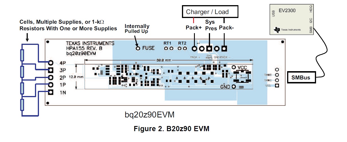
I made a simplified design, which have been tested on the Eval bord without problem

:7610.C BB-P030200-SCM.pdf

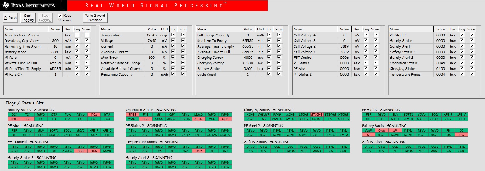
Now I can charge the battery, with both FET turned ON.

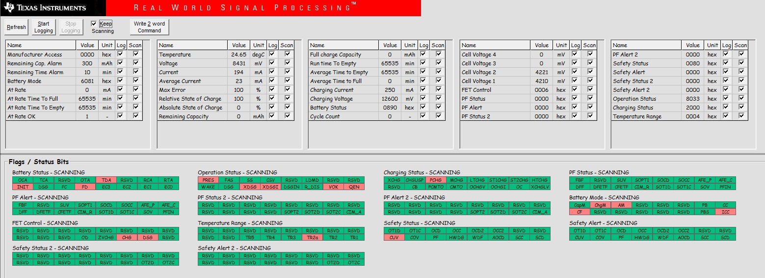
The problem is when I disconnect the charger. The DSC FET is turned OFF, and 2 errors flags are set:

XDSG and XDSGI

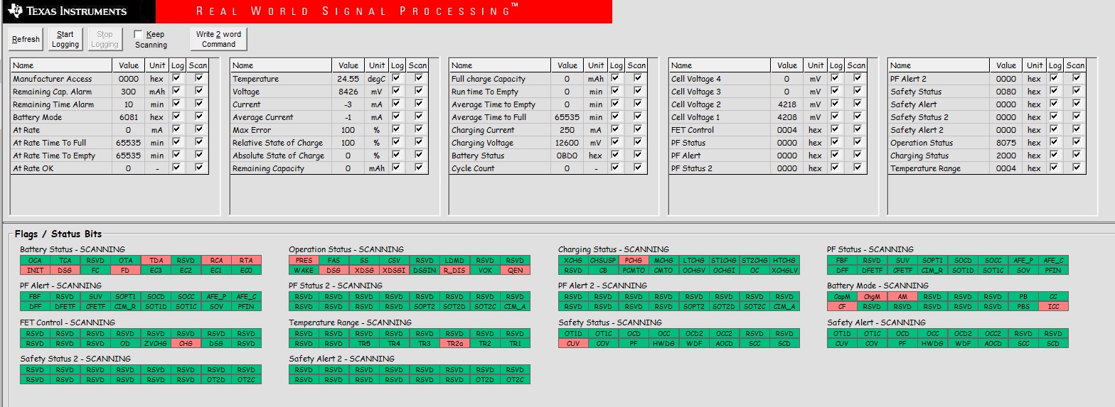
To be accurate, with no load, I can read 16V for 1sec, 5.4V for 1 sec, and then 0V. With a load, I read just few mV.

Any idea to help us for this projet ?

Thanks in advance.

Eric

  • Hello Eric,

    From your screen shots, I see the CUV bit is set in the safety status indicating that one of your cells is below the threshold set. Did you configure your device for 2 cells by setting the appropriate bits in the operation cfg A register in the data flash? CC1 should be clear and CC0 should be set.


    thanks

    Onyx

  • Hi

    Thanks for your help.

    I reloaded the flash with the from from my configured EVM module, and I no longer have these error flags.

    The actual problem now, on all prototypes, I don"t have a good voltage on the DSG pin. I read only 5.4V, and 6.2V if the R22 between DSG pin 1 and the gate of Q4 is disconnected, which is not enough for the discharge FET.

    I have the correct voltage on the charge FET (16V).

    Is there some SW issue, or maybe RoHS soldering temperature problem?

    Eric

  • Hi Eric,

    Clearly this will not be a SW issue. What does the voltage on the EVM measure? The simplest and first debug process will be to compare your circuit to that of the EVM. If they necessary sections are exact, try replacing/reflowing the solder on one of the ICs and see if that helps

    thanks

    Onyx

  • On the EVM, I read 17V on each FET gate.

    The bq20z65 has been changed, with the same problem. 5V on pin DSG when teh DSG FET is turned on.

    Any idea?

    Eric

  • How much different from the evm reference schematic is yours? Pls compare the necessary sections  of the schematic. What fets are you using?

  • Very few. No 2nd protection, no LEDs and no precharge FET . Here is the SCH file.

    0830.C BB-P030200-SCM.pdf

  • hi Eric,

    I looked over your circuit and it looks very similar to the EVM schematic with the exception  of your grounding. The SMbus, pack- lines out to be connected to chasis ground while the rest of the ground ought to be connected to VSS. Both grounds then ought to be tied at the sense resistor. For your schematic, you have all the grounds as one commond ground.That's the only thing that stands out in your circuit. Do you currently have a load or charger connected to the pack pins? Try disconnecting, though and see if you can have your data and clock ground separated from the other grounds. I don't see how/why having your ground connections as is on your design will cause the dsg pin voltage to stay at the ~5V which you are seeing but it is worth giving it a shot.


    thanks

    Onyx

  • I'm wondering If the procedure to activate the chip is to connect 2 R 1k before connecting the LiPo cells.

    I mean something in the activation procedure which can damage the chip.

    Difficult to to try your proposal without making a new design. By the way, even if the SMBus is not connected, we still have 6.2V..

    The datasheet gives V(DSGON)= V(DSG) - V(PACK); is between 8 and 16V.

    BR

    Eric

  • I am confused by what you mean by "connect 2 R 1k".

    The procedure to wake the device up is application a voltage on the pack pin. A value around 4.5 V thereabout.


    thanks

    Onyx

  • The EVM modules have been activated with the following:

    using 1k resistances.

    Our prototypes have been connected directly to LiPo celles, Low voltage  first, High voltage 2nd, and then activated with a 8V PSU.

    Thanks

    Eric

  • Oh no!! you misunderstood what the EVM user guide was explaining. It means you are to use either resistor strings and a power supply to simulate cells or actual cells. You are not to use the cells and a power supply. That should be the reason your dsg pin is acting up.


    thanks

    Onyx

  • My last experiment was to take the chip from the EVM module which works fine, and solder it on the prototype.

    I still have the same problem, so I suppose that something in the electronic diagram is wrong.

    Any idea?

    Thanks

    Eric

  • Now take a chip from one of your boards and place on the EVM. If the voltage on the dsg pin is normal, i.e 10V there about then we can say with certainty something on your board is clamping the voltage to 5V. On the other hand, the pin could already be damaged and then you will see 5 V on the EVM regardless. You will have to debug/prod your board to see what the cause is. If the EVM with a chip for your board behaves right, you can use it for comparison. Measure voltages around your circuit components and compare to the EVM.


    thanks

    Onyx

  • Ok I will do shortly.

    By the way, I read on other post some advice about unused pins, like FUSE and /PFIN.

    In my design, they are just not connected.

    1682.0830.C BB-P030200-SCM.pdf

    In this other post, it's recommended to ground the SAFE pin through a 200k resistance, and PFIN connected to 2.5V via R 5.1k.

    0434.bq20z65_No2ndProt_NoFuse.pdf

    This difference could it be the cause of the DSG pin malfunction?

  • Hello

    I did what you said:

    I start with and EVM module which works fine, and a prototype, which have not enough voltage on the DSG pin

    1) I move the chip from the EVM to my prototype:

     The same issue is observed.  Only 5.5V on the DSG pin

    2) I move the chip from a prototype to the EVM module:

    The chip works fine. we have 16V on the DSG pin.

    As we could observe, When we charge battery, from 4.5V on PACK pins, the charge pump of the discharge pin starts to works, and we have enough voltage to activate the pin, but only in this case.

    Is there something in the software, or in the design that could disturb the DSG charge pump?

    I also measured all the voltage on all points. No difference between EVM and the prototype, but the DSG pin and the PACK pin (5V)

    BR

    Eric

  • Hello Eric,

    I have figured out the cause of your problem. You have R24 populated on your board. On the EVM, the 100k resistor is DNP. Take that off and your DSG pin will be work fine. The DSG FET charge pump is powered by the PACK pin and having the 100k prevents it from powering up.

    thanks

    Onyx

  • Hello Onyx

    I removed R24 on my board, without any change. Still 6V on the DSG PIN.

    As this is a critical point in our schedule, do you have any other idea to help us?

    This chip seemed very promising for us, but we have now very short time to launch the production, and we are now already looking for an alternative solution in case a failure of the bz20z65 solution.

    BR

    Eric

  • Hi Eric,

    I have sent you a friend request. We should be able to exchange private messages on there. Send your email and a contact number you can be reached at.I will set up a conference call to discuss this.

    thanks

    Onyx