This thread has been locked.

If you have a related question, please click the "Ask a related question" button in the top right corner. The newly created question will be automatically linked to this question.

PCB design verification required for charger BQ24192 for 20Ah,3.7V Li-Polymer

Other Parts Discussed in Thread: BQ24192

Hi,

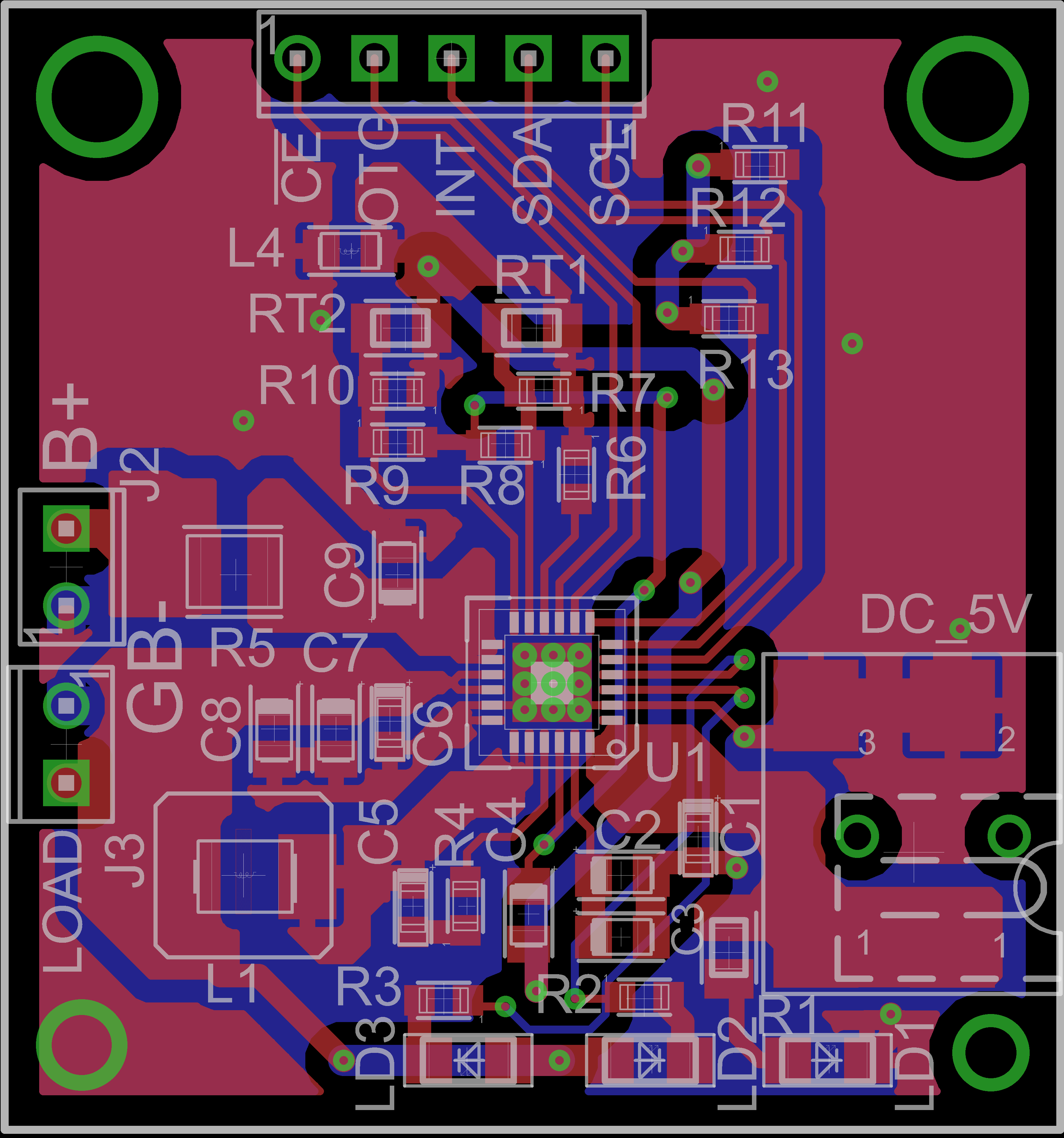
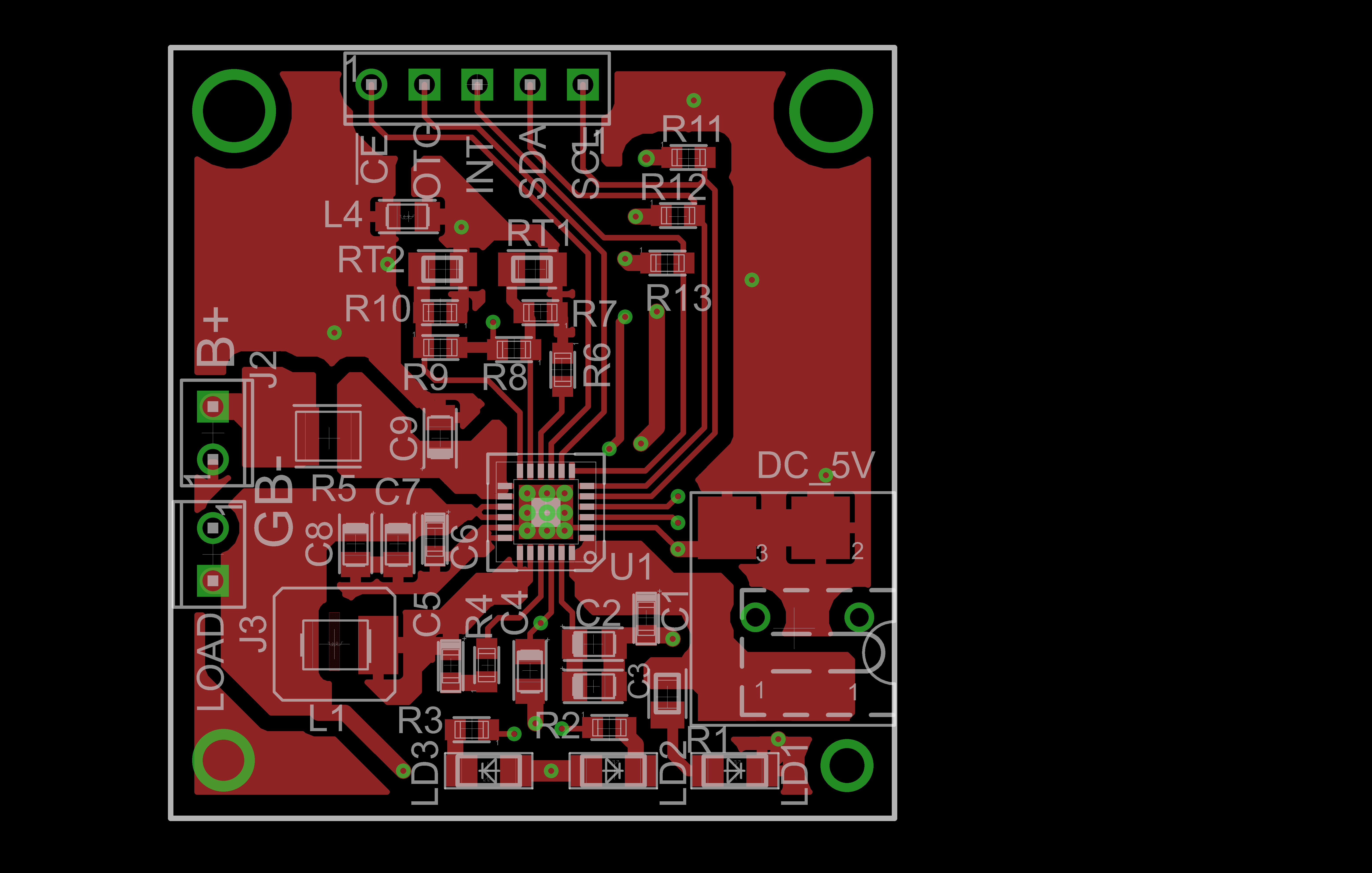
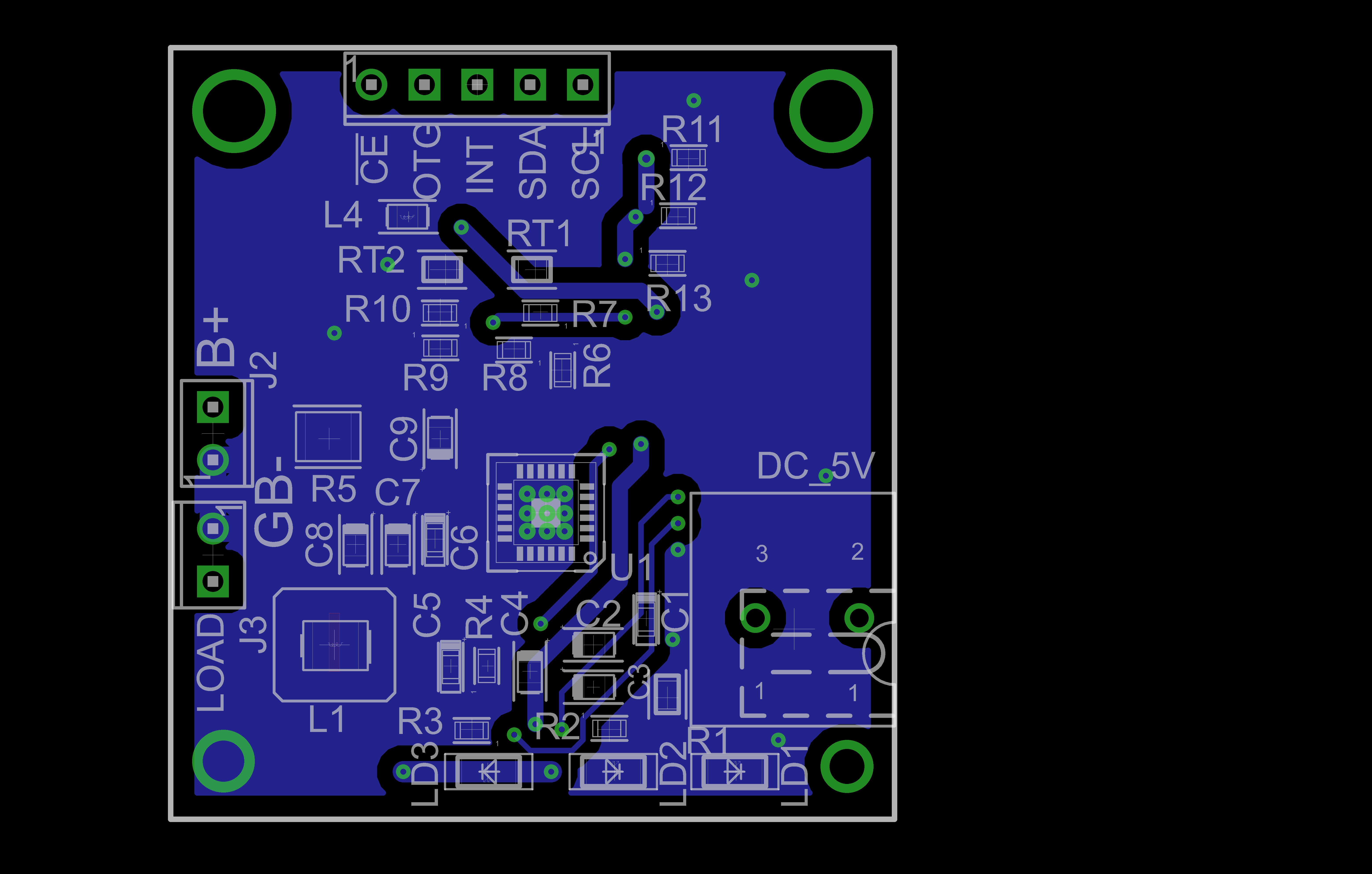
We are using BQ24192 charger IC for our 3.7V,20Ah Li-Poly battery application. I have referred TI evaluation layout design for our new design which is shown below. So please check and verify the design and Let me know any changes required for our new design. So that we can give it for PCB manufacturer.

Also Advice we need 4A/maximum charging current,So is there any changes required in this design?and How to achieve 4A/maximum current?

Regards,

Naveen K

  • The circuit and layout for the most part look ok and organized, but there are some things to be concerned about.

    The PCB looks very small (~25mm sq. or 1" sq) and probably is too small for 4A.  There will probably be around 2.3W of dissipation.  There is a direct correlation between board size (surface area) and temperature rise.  In a enclosed area with no air flow the temperature rise from ambient is around 125C per watt per inch squared.  In an enclosed area the ambient may be 50C and so the temp rise allowed may be 75C max.  This means that for 2.3W*125C/W/75C = 3.8 inches square.

    The design has 2 sq inches (one on top and one on the bottom).  It needs a minimum of 4 sq inches (two on top and two on bottom.

    Since this is a two layer, one has to be very careful to route the traces in the ground plane.  On the right hand side there are several traces next to the IC which effectively remove that side of the board for cooling.  A full ground plane on the bottom is very important since the IC is a quad package and there is no copper tied to the power pad on the top layer, so the only way to spead the heat out (conduction) is on the bottom layer.

    I do not know what thickness copper you are using but it should be 2oz.(0.07mm).

    I would fill in the power etches to the IC and not have the fingers (SW, GND SYS and BAT).


  • Thanks for your advice.

    The present board size is 1.3 inch x 1.4 inch. The copper thickness is  0.035mm FR4.

    1.We will add this layout to our system layout together. Then our system PCB size will be 142mm x 92mm. For this case can we add present charger layout to system layout without any issue? Please advice me if any changes required.

    2.We also need separate charger circuit. So if we increase board size to 4sq inches. can we achieve all consideration without any issue? Provide your Advice.

    3.Sorry i didn't understand"I would fill in the power etches to the IC and not have the fingers" Please advice in different way.

    4.Also advice can we eliminate thermal relief for the IC thermal pads for proper heat transfer? Is there any issue? 

    Regards,

    Naveen K


  • A1) It is good the board will be bigger, but with a 4A charger there will  be ~2.3W of dissipation and it is best to have as much copper to spread the heat out as possible. If you can only have 0.035mm thick then I would have two full layers and minimize the routing in the copper plane that cuts off the heat flow.  The amout of copper, size and heat dissipation are directly related to temperature rise.

    A2) 4 sq inches for 2.3W is probably a minimum.  A larger area is better, thicker copper is better and less heat dissipation is better. 

    A3) I typically have a copper pour between the two power pins so the connection resistance to the IC is better.

    A4) I typically do not use the thermal relief (finger connections to the component), because I like the lower resistance and better thermal connection.  Does not see to matter for a automatic flow where the whole board is heated, but it does make hand repairs harder to unsolder the components.

  • Thank you very much for your information. We will appreciate your support.

    Best Regards,

    Naveen K