This thread has been locked.

If you have a related question, please click the "Ask a related question" button in the top right corner. The newly created question will be automatically linked to this question.

PCB design verification required for regulator TPS54327

Other Parts Discussed in Thread: TPS54327

Hi,

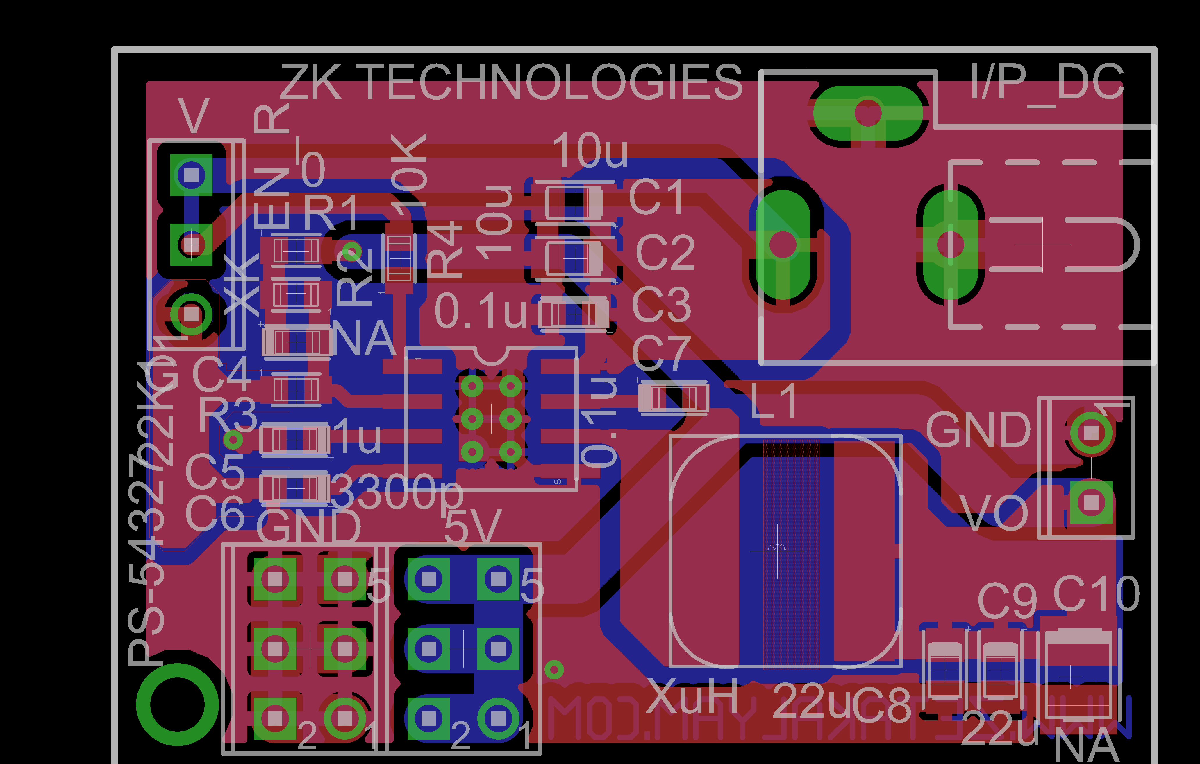
We are using TPS54327 SWITCHING REGULATOR(Adjustable type(i/p=13V and o/p=3.3 to 5V) so some resistors values are mentioned as X and we will choose it from EVM datasheet table) for our device. I have referred TI evaluation layout design for our new design which is shown below. EN pin is shorted to Vin for enable the device. So please check and verify the design and Let me know any changes required for our new design. So that we can give it for PCB manufacturer.

Regards,

Naveen K

  • I'll try to check it tomorrow.  I have a rather full queue leading into the holiday season.

  • I would rotate the inductor by 90 degrees clockwise and place output capacitors close to the IC to minimize ground current loop.

  • Yes the layout is generally quite good.  I agree with the previous poster.  You may get somewhat better performance by minimizing the circulating current path in the output.  It will depend on your requirements for placing the output connector.  One other issue is the routing of the ground connection for the output.  While your Vout connector attaches directly to the VOUT copper area, the ground connection takes a circuitous path back around the top of the board.  it would be better of it connected directly to the ground side of the output capacitors.  You could move C7 closer to the IC, then move L! slightly left and up.  For TPS54327 there is probably no need for your C10 (it looks like pads only, no component) and you could place your output connector there,  Moving L1 up would allow for a wider ground return trace as well.  I would consider that more critical than the above post.

  • I would definitely eliminate thermal relief connections from the IC's thermal pad to the ground polygon. Thermal relief connections are necessary to prevent tombstone effects for small fine-pitch parts and excessive heat leakage while soldering manually. None of these applies to your case.

    Also you should always use direct connection of polygons/planes to vias. Nothing is gonna be soldered to vias anyway.

  • Thanks for your Advice, Yes you are right, as per our requirement we cant place the L in vertically. We added C10(optional) for using high value capacitor/ for tantalum type. We will add this layout in to our system layout and we will connect Vout and o/p capacitor ground pads directly to the system load, so we can avoid the ground loop in output side right?

    As per your advice, please check and verify the modified layout for this individual board.

    Regards,

    Naveen K

  • Thanks for your advice,

    If we eliminate the thermal relief it may chance to dry solder or it may not give proper connectivity(because of bad soldering) right? Is there any issues when we give it for re-flow soldering?

    "Direct connection of Polygons/planes to vias" means have to use dummy vias for airflow/ connecting top and botum polygons right? If not please advice in other way.

    Regards,

    Naveen K

  • Loops to the load are not really that critical and that tantalum capacitor won't make any difference. What is important is to eliminate next loops (see the picture) as much as possile.

  • If you use reflow soldering there should be no problems with direct connections of thermal pads to polygons/planes. By using relief connections for preventing heat leakage during manual soldering you jeopardize the main idea thermal pads designed for - taking heat away during normal operation.

  • I don't have a big problem with thermal relief on component pads, but you definitely want to avoid them under the IC for the thermal pad connection and to connect the copper on the top and bottom side ground.  Make sure the via hole sizes are small too.  i think we use 10 0r 12 mil vias to prevent solder wicking.  I'm not sure about adding that ground trace to the output connector.  You essentially have two parallel return paths back to the IC.  It will probably work, but I would not design it that way.  You might as well do it as I suggested.  C10 is not recommended for DCAP2 topology.  DCAP2 is designed to work nest with low ESR types such as ceramics.  So you could place the output connector where C10 is currently located.  As the ither poster pointed out the green loop is the most critical, but for good design practice I like to minimize the other loop as well.  The VOUT and GND portions are not too critical, but you definitely want to be careful with the switching node.

  • Thank you very much for your suggestions.This is the modified board as per your suggestion and other post. Yes this is correct for thermal pads,But i thought thermal relief pads is sufficient to heat spread. Thanks for your advice about this.

    I want one more clarification regarding to select the capacitor voltage. Is there any advantage /disadvantage if we choose higher voltage rated capacitor(:example if application requires 10V rated capacitor i will use 25V or 50V rated capacitor)?.Please Advice.

    Regards,

    Naveen K 

  • Thanks for your suggestions. Know i understand about thermal relief v/s thermal pad. I posted modified layout file.

    Best Regards,

    Naveen K

  • That layout seems good.  About the capacitor voltage, ceramic capacitors have reduced capacitance as the applied dc voltage increases towards the rated voltage.  The amount of reduction can be surprisingly high.  For output filter caps, I typically use at least 10V rated caps, even for low voltages like 2.5 V.  For input voltage it becomes more difficult, so I use the highest voltage practical, then if the maximum input voltage is close to the rated voltage, I use 2 input caps instead of 1.

  • Thanks for your advice, 'typically use at least 10V rated caps, even for low voltages like 2.5 V' means there is restriction to choose minimum voltage rating(like 10V) but no restriction to use high voltage rated capacitor say 25v or 50V for 2.5V right?

    Why am asking this because for some application we are using 25V/50V rated capacitors, but in some datasheet(TI) they recommend to use 6.3V/10V rated capacitor.If we use present capacitors(25v/50V) we can avoid to buy another voltage rating(6.3v/10V). So whats your suggestion?we can use 25v/50V for all application like 2.5V/5V power application or we need to use both voltage rating like 6.3V,10v,25V for different purpose.

    Except capacitance is there any other issues like efficiency drops ?

    Regards,

    Naveen K

  • I think the main trade off here is size.  For example take 22 uF X5R.  For 25 V rating it may only be available in 1206 or 1210 case size.  For 0603 case size, you can only get 4V or 6.3 V rating.

  • Double and triple voltage rating for capacitors came from tantalum once. They really require higher voltage rating to withstand high-temperature environment. For ceramic capacitors you can easily go away with using 6.3V capacitors for 5V rails and 4V capacitors for 3.3V rails (but for the purpose of unification I always use 6.3V capacitors though).

    What is important is not to go the smallest available size. Capacitance rating is only true without DC bias. Once you apply DC bias your capacitance could drop 50% and even more. And increasing rated voltage doesn't make any difference. Size is what matters. Take a look at the pictures below for 6.3V 22uF X5R ceramic capacitors in 0603, 0805, 1206 and 1210 packages from Murata (the pictures are similar for capacitors form any vendor). At 5V DC the efficient capacitance is only about 20% of original one for 0603 case and 70% for 1210! Increasing the rated voltage doesn't really change anything.

  • Thank you very much for your advice. We will appreciate your Support.

    Best Regards,

    Naveen K

  • Thanks for your information. Yes i agree with your words, for some values capacitors size is proportional to capacitans and voltage rating.Except operating temperature is there any other difference between X7R and X5R ?

    Regards,

    Naveen K