


Hi everybody, and happy new year.
I’m a beginner, so please forgive me if I write something stupid; before writing, I’ve read others threads in this forum about the expression “it is recommended that the board be designed with separate ground planes for VIN and VOUT, with each ground plane connected only at the GND pin of the device” that can be found in many LDO regulators datasheets, but I’m not sure to have well understood.
My project is based on a MSP430G2553, in QFN package; few weeks ago, I wrote in the MSP430 forum, to have indication about the proper layout.
The supply voltage comes from a 3V battery, regulated by an LDO (2.5V).
In the picture below, you can see the result.

I’m planning to use even an OpAmp to amplify an analog input, and it will be connected (GND) to the ground end of the output capacitor of the LDO (C1), as well as any other component will be connected to that point.
Now; I’m planning to use, as LDO, the TPS78225 in SOT23 package, so I need to change the picture.
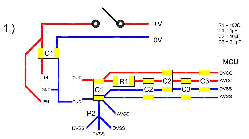
You can see that the ground end of the output capacitor of the LDO is the ground star point, while P2 is a secondary ground star point for all digital grounds.
I’m planning to use this LDO for its very low Iq; in my application, the power consumption will never be above 1mA.
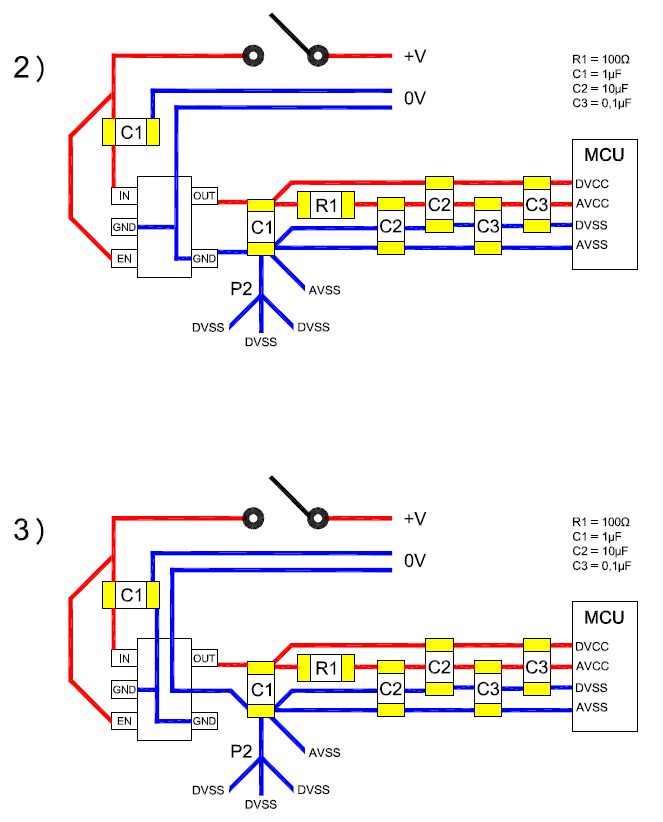
Considering that it will be important to have a good output noise from the LDO, do I have to change something, considering that “it is recommended that the board be designed with separate ground planes for VIN and VOUT, with each ground plane connected only at the GND pin of the device” ? Maybe the following layouts would work better?
Another question; if I use the same LDO in SON package, how am I supposed to connect the thermal pad to ground?
Thanks in advance to everybody.
Marco
