This thread has been locked.

If you have a related question, please click the "Ask a related question" button in the top right corner. The newly created question will be automatically linked to this question.

LM3478 switching noise

Other Parts Discussed in Thread: LM3478, CSD17308Q3

Hi all,

I designed a boost converter based on LM3478 using webench.

Main characteristics are:

Vin=12V

Vout=19V

Iout max=2.5A

8547.webench_design_1126287_25_189261659.pdf

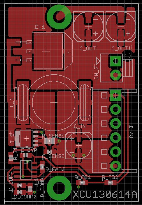
I slightly adjust webench component values to obtain the following schematic:

My problem is after receiving prototype, I measure huge switching noise.

Have look at oscilloscope screen:

CH1 Vout

CH2 Vin

Output current 1A

6087.Vin_Vout_Iout-1A.tif

CH1 Vgs

CH2 Vds

Output current 1A

8156.Vgs_Vds_Iout-1A.tif

I know Csense should be directly connected to Isense pin. So I tried shorting RS1 but nothing changed.

Current limit doesn’t work (at 3A output converter still provide 19V).

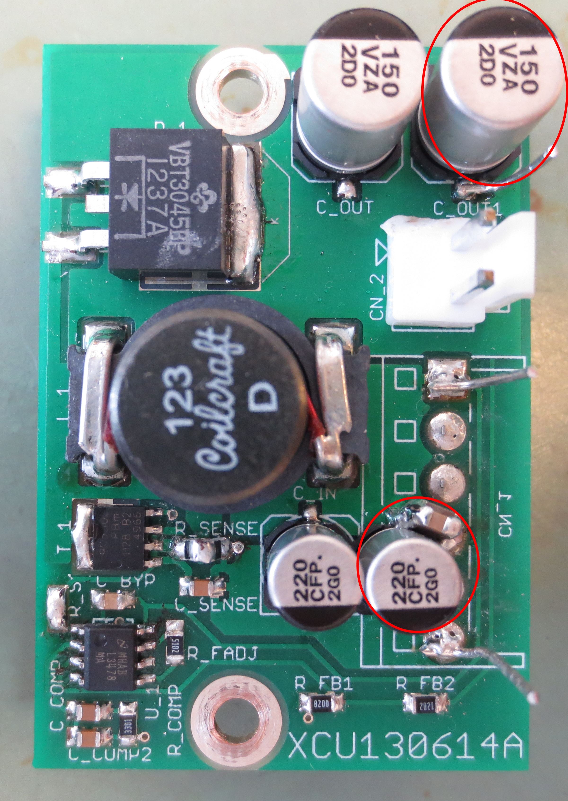
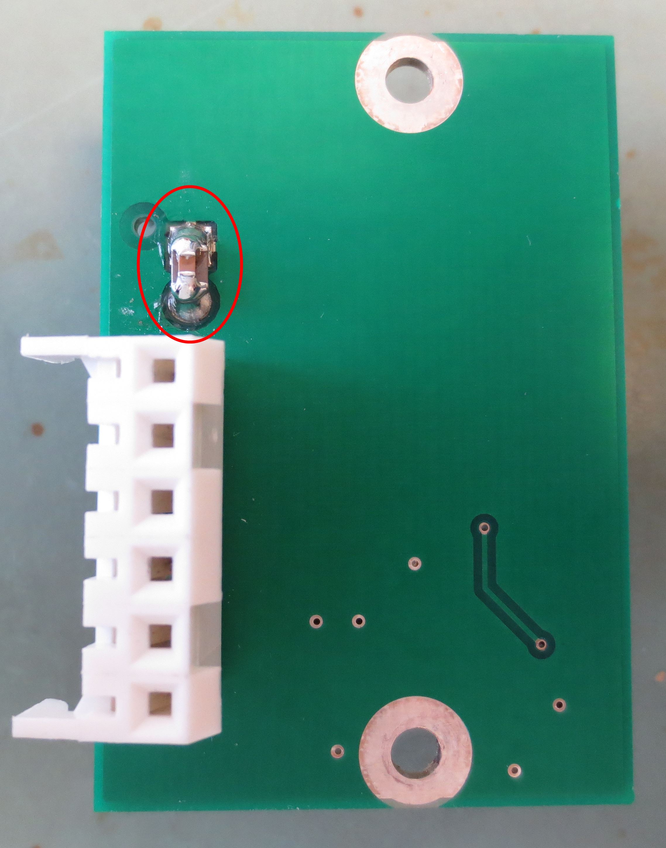
Does the problem come from BOM or PCB layout?

Many thanks in advance.

  • Hi,

    Question 1.  Noise.  This type of high frequency noise is usually due to layout.  On a boost converter the important loop is between the the FET drain -> diode -> output cap -> and the FET source.  Try to make this loop as tight as possible.  Look at adding some x5r or x7r 0.1 to 1uF ceramic capacitors to the output as close to the source of the fet and the diode as possible.


    Question 2.  There can be variation in the current limit due to mosfet on resistance and other factors.  If the on resistance of the FET is lower than expeced this would lead to a high current limit.  Try adjusting the limit down.


    Regards,

    Marc


  • Hi Marc,

    Thank you for your quick answer!

    Qusestion 1: Noise

    As you can see on following pictures I doubled input and output electrolytic capacitors and added stacked ceramic X7R capacitors (100nF + 2.2µF):

    With these additional capacitors switching noise is lower:

    CH1 Vout, CH2 Vin, Output current 1A:

    CH1 Vgs, CH2 Vds, Output current 1A:

    If necessary have a look at PCB layout:

    I assume critical path is right, isn’t it?

    How to improve noise immunity?

    Qusestion 2: current limit

    I doubled Rsense value (from 12mhom to 24mhom). Using 12mhom, duty cycle starts decrease from 4.5A. With 24mhom, duty cycle starts decrease from 2.2A

    So it is better, but I don’t know why exactly as Rdson of these 2 MOSFET (CSD17308Q3: webench; PSMN9R5-30YLC: used) are almost the same.

    Before measuring I thought that in case current limit was reached, the output voltage would drop immediately to 0V. But actually the duty cycle is gradually reduced.

    Could you confirm?

    Moreover I suppose changing Rsense must involve compensation slope adjustments. Is-that right?

    Best regards

  • =Same message pictures uploaded correctly=

    Hi Marc,

    Thank you for your quick answer!

    Qusestion 1: Noise

    As you can see on following pictures I doubled input and output electrolytic capacitors and added stacked ceramic X7R capacitors (100nF + 2.2µF):

    With these additional capacitors switching noise is lower:

    CH1 Vout, CH2 Vin, Output current 1A:

    CH1 Vgs, CH2 Vds, Output current 1A:

    If necessary have a look at PCB layout:

    I assume critical path is right, isn’t it?

    How to improve noise immunity?

    Qusestion 2: current limit

    I doubled Rsense value (from 12mhom to 24mhom). Using 12mhom, duty cycle starts decrease from 4.5A. With 24mhom, duty cycle starts decrease from 2.2A

    So it is better, but I don’t know why exactly as Rdson of these 2 MOSFET (CSD17308Q3: webench; PSMN9R5-30YLC: used) are almost the same.

    7345.MOSFET_CSD17308Q3.pdf

    8688.MOSFET_PSMN9R5-30YLC.pdf

    Before measuring I thought that in case current limit was reached, the output voltage would drop immediately to 0V. But actually the duty cycle is gradually reduced.

    Could you confirm?

    Moreover I suppose changing Rsense must involve compensation slope adjustments. Is-that right?

    Best regards

  • Critical loop is high light above.  You want to place the ceramics as close to the bottom of the sense resistor as possible to filter high frequency noise. 

  • 2) Current limit

    Yes the out put voltage will be gradually reduced as the current limit for the part is actually more of an output power limiter. 

    You will need to recheck your compensation.  You can use (SNVA067) as a resource.


    Marc