This thread has been locked.

If you have a related question, please click the "Ask a related question" button in the top right corner. The newly created question will be automatically linked to this question.

Trouble with LM25085

Other Parts Discussed in Thread: LM25085

Hello,
I used Workbench Design Center for a buck regulator with this characteristics :

Vin : 6.5V to 9V   |   Vout : 6V 3A   |   Ambient temp : 20°C

It gave me a design with the LM25085, then I ordered the necessary components and tried it in dead-bug prototyping. But after quick tests without load I observed a characteristic curve which doesn't correspond to what I was expecting.

There is 4 point :

1. in every case, the output tension is not stabilized at 6V

2. between 6.5V and 7.8V on input tension, the signal is disturbed at the output

3. above 7.8Volts there is no more noise but it is still not stabilized at 6V

4. when I put a load on the output (resistor 6W 22Ohms), the tension collapsed

Can you tell me if this schematic is possible? I tried to use the closest components adviced in the BOM. Maybe some of them doesn't work for this case...

  • Your images do not seem to be showing.  Can you re-post them?

  • Weird, I saw the preview when I posted the topic...

    in .rar maybe..?

    2330.screenshots.rar

  • Hi Olivier,

    I cannot open the .rar file. Please post the images. I am not sure deadbugging a switcher is a good idea. The LM25085 evaluation board is probably the best place to start.

    Thanks and regards,

  • I have Winzip on my computer and extracted the .rar files.   I will send them to Vijay by email.

  • Thank you David for helping unzip the files.

    The VIN/VOUT waveforms are not very helpful in figuring out what is wrong with the board. Is it possible to send the SW node waveforms and the inductor current waveforms?

    Also it will help to print and attach the webench design document. From the RON/VOUT value it seems like it is a 600kHz design. Sense resistors need to be placed and routed properly as they are noise sensitive. In addition, the diode is 2A which is below the max load current. It should be rated for 3A.

  • Hello guys,

    Thank you for your responses. And particulary to David who sent the screenshots.

    The LM25085 evaluation board seems to be very fine, but it costs 75€ without postage charges (France) so I'm just going to use the same design :-).

    I think I'm going to change the set resistor + capacitor which determine the current limit by keeping the same from the evaluation board (1000pF and 2.05K). Then I'm going to change the inductor to 15 uH. what do you think ?

    Concerning the sense resistor, what do you mean by "Sense resistors need to be placed and routed properly" ? I think it needs to be change by a 10mΩ.

    Did you meant PGATE when you said SW node ? I'll do other mesures as soon I finished to change all this stuff. Then I'll post you the new screenshots.

    Finally I'll see if I have a diode rated for 3A.

    I join you the webench design document.
    8228.webench_design_3515386_15_928124614.pdf
    Thanks.

  • hello again,

    So, I changed the components I described on the last post, except for the diode (still at 2A). Plus, notice I change the inductor for 15uH see the link : http://docs-europe.electrocomponents.com/webdocs/0fe1/0900766b80fe1f3e.pdf

    The good new, there is an amelioration : between 6.5V and 7.8V, the output signal has less noise as before.
    The bad ones : the output signal is still not stabilised at 6V and with a load the tension still collapse.


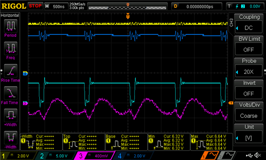
    First, 6.5 Vin and unload

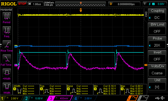
    second, 6Vin with load (warning period changes)

  • Hello Oliver,

    I am having difficulty understanding the 6V waveforms with load when you say the output tension collapses.  Could you label the wavforms?   If the output collapes the FB pin should follow to a low level and the PFET switch should conduct 100% of the time.  This will increase the current in the inductor until current limit threshold is reached.  The current limit circuit will turn off the PFET for a time which is dependent on Vin and FB votlage as described in the datasheet.   If you ar ereaching current limit, then the Radj resistor can be increased. 

  • OK,

    for the labels, look at the right you have the different 0V references:

    Vin (CH1) and Vout (CH4) are superimposed

    Vpgate (CH2) and Iinductor (CH3) are superimposed too. (CH3 has a differential probe)


    Otherwise, I already understood how the device works, but no matter, thanks to confirm what I thought.
     So you advice me to increase the value of Radj ? As I said at the beginning of the topic I changed the initial value (2.55kΩ) for the same rated in the evalutation board (2.05kΩ).