This thread has been locked.

If you have a related question, please click the "Ask a related question" button in the top right corner. The newly created question will be automatically linked to this question.

UCD90120A GPIOs behaving badly

Other Parts Discussed in Thread: UCD90120A

I have two GPIO pins defined as A=B&!C&!D E=B&!C&!D.

Most of the time these function correctly, but I have found multiple times them getting stuck in the state where B is high, C and D are both low, but A and E are also low. (B, C, & D are also GPIO pins).

Once in this state they continue to behave this way until the IC is reset.

I don't know how to trigger this behavior, but this has happened often enough that I have been able to connect the USB Interface Adapter and us the "GPIO pins peek/poke" window to verify this incorrect behavior.

Is there some way to make this work reliably? Is there a way to detect and recover from this state using the I2C without resetting the IC?

  • I have another instance where logic drives an LED. When I set up the logic and write to ram, it works, when I save it to prom and reset the IC it no-longer works

    I have been able to reproduce this behavior on the demo board.

    Sequence to reproduce:

    edit AllGood pin, change the enable state on "NOT PWR_OK (pin 14)" make sure "not" is checked. (this assumes that pin 14 floats low) (it is necessary to change something in the logic to be able to write to the RAM of the IC)

    Write to Hardware, note that LED D17 lights up.

    Store RAM to Flash

    push the reset button, note that D17 goes out.

    Bring up "GPIO Pins Peek/Poke" page, note that all pins read "Low"

    Verify logic on AllGood signal and see that if all its inputs are low, its output should be high, but it isn't.

    .2133.UCD90120A @ Address 101d Project.xml

  • GPIO pin numbers: 10, 36, 37, 38, 39, 40 are for JTAG interface. If the board has the PMBus address = 126, that for JTAG use and those GPIO pins might not function correctly. Either change the device's address (see http://www.ti.com/lit/ds/symlink/ucd90120a.pdf, section PMBus Address Selection, for more detail) or use other GPIO pins

  • The address I am using is 0x37, or 55 decimal. The JTAG interface is not enabled.

    In the demo board example I created, I had the address set at the default of 101  (jumpers in positions 1-2 and 7-8). JTAG is also not enabled in this case.

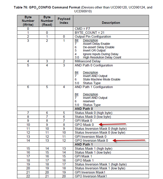
  • I import the configuration to the device using the project file (2133.UCD90120A @ Address 101 Project..xml) that you provide, when I read the GPO_CONFIG for GPO #7 (WriteByte code = 0xF7, value = 0x06; then follow by ReadBlock code = 0xF8), I get back the configuration for the GPO #7 (GPIO14, Pin #29, name = AllGood) as:

    66000000130000007F0000007F0000000000000000

    Byte[8] and byte[12] are for GPO mask and GPO Inversion mask for AND PATH 0 (UCD90XX PMBus Command Reference), according to the config, GPO 7 is set to depend on itself => that is why the logic is not reliable (GPO config should not rely on itself for logic output)

    Change the GPO_CONFIG for GPO7 to 0x66000000000000001F0000001F0000000000000000


  • I am using "Fusion Digital Power Designer" to edit the GPIO logic.

    This tool does not give me the option to select or de-select pin 29 as an input to the logic of pin 29, though I do see that it is being used. I will attempt to delete the pin and re-create it to see if I can get that input removed.

    Perhaps this explains the extra input wire going to the title bar in the "GPO-Pin29 DBG_GPIO14 - AND Path #1" window.

    In any case, there is a bug in the GUI that allows a feedback loop (probably initiated by using the "Move Selected Pins Up" or "Move Selected Pins Down" function on the pin assignment page.

    A quick test shows that deleting the pin and re-creating it seems to fix the problem. I will now go check to see if the other instances of flaky behavior are caused by the same issue.


    Thanks

  • I went and updated the logic on my board for the power good issue, and this has been fixed.

    Unfortunately the issue in the 1st post of this thread is not the same as this one. It does not have a feedback loop. Worse, I don't know how to make it repeat.

    Attached is the design with this issue. The affected pins are: "Aud_En0 and Aud_En1.

    Usually they work, but sometimes they get stuck in a nonworking state. They both fail together. (If one is not working, the other is also not working). Once not working, they remain that way until the IC is reset.

    The attatched version of the file is known to have the issue. I have created a new version that moved some stuff around in hopes of avoiding the problem, but I have not used the new version enough to know if it avoids the problem.

    0830.Labyrinth 52d Rev B Bad.xml

  • Can you describe what does not work? I tested on my board and it works as expected

  • This is an intermittent problem that I don't know how to trigger.

    When it is in a bad state, the outputs do not go high even though the inputs are in a state which should cause the outputs to go high.