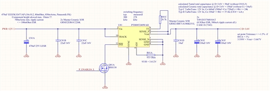
I'm using a PTH08T240W on a 125MSPS ADC Board to power FPGA and other components.
Therefore I need preferably less ripple at power rails to get a clean FFT spectrum from ADC data.
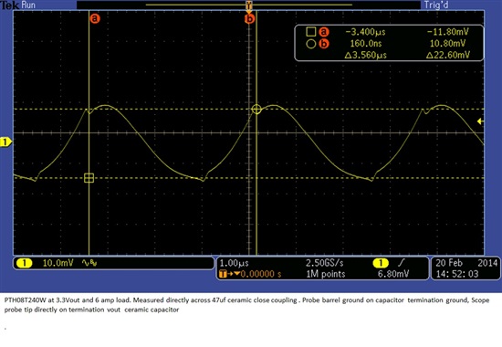
Datasheet states a Vo ripple of typ. 10mVpp (20MHz BW).
Input of circuit is 12V and output 3.6V.
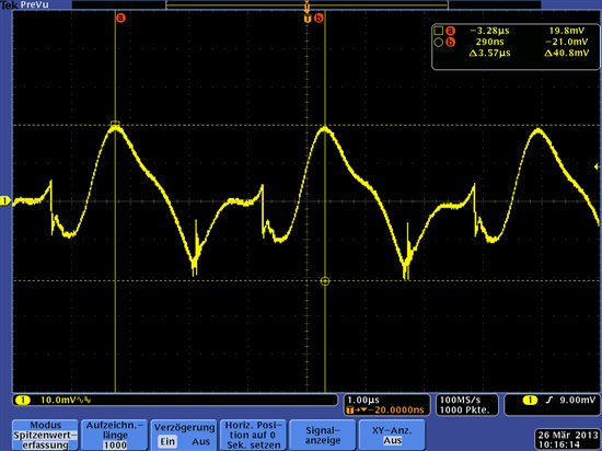
I have measured output ripple with scope BW limited to 20MHz and a probe with short GND tip.
Output ripple measured is around 40mVpp.
What in my schematic or pcb design can be wrong resulting in increased Output ripple?
Here my schematic and scopeshot from measurement.
best regards
Andreas


