This thread has been locked.

If you have a related question, please click the "Ask a related question" button in the top right corner. The newly created question will be automatically linked to this question.

No Load Leakage with TPS40054

Other Parts Discussed in Thread: TPS40054

We aren't sure what's happening with the TPS40054.

Basic design:  35-38V input

Output: 12-30V

Max power out: 150W

Problem:  When the controller is forced off (using SS).  And there is no load our output voltage creeps way up.  We've tracked it down to leakage current going into the boost pin of the TPS40054 (~1.7mA).  On new parts, this seems to be around 4-5V (<<1.7mA) which we consider to be OK) , but on a few boards we have seen this be 18V (~1.7mA into boost pin) which is unacceptable.  This has been intermittent and we can't narrow it down to a certain condition that causes it.  The only thing that fixes the issue is to replace the TPS40054 chip... 

The boards where this has occurred have been handled quite a bit as they are prototypes; so, we think static might be an issue, but we want to rule out any major issues.

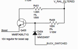
Note:  We had to add a secondary charging circuit for the boost cap due to the high output voltage (30V).  Otherwise low load regulation isn't possible with the TPS40054 alone (which of course is not anywhere in the spec sheet).  The circuit charges the cap to 10V over the switched node voltage and doesn't require the switched node to be zero volts (which the TPS40054 requires for higher output voltage).   We believe this could also be causing it, but the circuit is same across a bunch of boards with only a relative few problems and all the boards have been heavily stressed.

Any thoughts?  The only one we have is to replace the 10V regulation with something lower... like 9V or 8V...  

Thanks,

Kyle Miller

  • Kyle,

    Can you post the section of the schematic that includes the external secondary charging circuit for the BOOT cap? Is this charging circuit a floating supply or ground referenced?

    I will need to consult with design to see if there is some sort of voltage clamp on the boot voltage, although I doubt there is. Keep in mind that the majority of DC bias current that enters the BOOST terminal will exit the SW terminal, and this is expected and is how the internal boot and high drive circuit are designed. This bias current will directly charge the output bus when there is no load and no switching.

    Regards,

    MC.

  • I realize that this current will exit the sw terminal.  The problem is that this is changing.  New ICs and good ones will take in about 50uA into the boost pin (when buck is off), whereas, the boards that we deemed have "failed" are around 1.7mA in the same condition.  I want to know what might be causing this and what I might be able to do to fix it or prevent it.

    "Vrail_filtered" is just Vin past a small low pass filter, "Boost" is the the "Boost Pin" of the TPS40054, and "Buck_Switched"  switched node of the buck which is also the "SW" pin on the TPS40054.  Also, note there is a 10 ohm resistor between the boot cap and the boost pin.

    Thanks,

    Kyle

  • Kyle,

    I've discussed this with design and there is no deliberate voltage clamp on the BOOT voltage. There are ESD structures within the device that if damaged could leak current. The normal bias current into BOOT and therefore exiting SW is in the order of micro-amps, so 1.7mA does indicate a problem.

    There are a few things you can try. First, unrelated to any failures, you might want to drop the zener voltage down a bit so that your external BOOT charge circuit isn't always supplying the BOOT current. You may only want it to kick in when there is no switching due to no load, and the BOOT cap starts to discharge. If your external regulator is set too high, it will be doing all the work instead of the internal BP10 regulator. No difference in efficiency, just a shift of the dissipation from the BJT to the device.

    Once you drop the zener to sub 9V, check a failed device. If it still sources 1.7mA from SW then likely the high driver has been damaged. If this is the case you can send the device in for FA, but this sounds most likely from your data.

    Another point of note, the MMBTA06 has only a 4V abs max rating from Emitter to Base (based on the Fairchild datasheet). When there is an active SW pulse, there could be more than this 4V from E to B depending on the capacitance of the zener (and how long it holds the 10V when SW is high). So you might want to check that the BJT isn't being overstressed. Any potential breakdown current will be limited by the 100k, but you may want to verify the stress.

    Regards,

    MC.

  • We'll be trying lowering the zener to 8.2V next week when we get parts.  The BJT part, I'll double check the actual part stress, but replacing that part didn't help the problem, so I believe the issue is still with the TI chip.  I'll update you when I have more information.

    I also don't mind the charge current going through the BJT as it far over rated for that purpose.  Hopefully, the 8.2V zener and better ESD practices will fix the issue.

    Thanks,

    Kyle.