This thread has been locked.

If you have a related question, please click the "Ask a related question" button in the top right corner. The newly created question will be automatically linked to this question.

LM22672-5.0 Faulting Issue

Other Parts Discussed in Thread: LM22672

Hi,


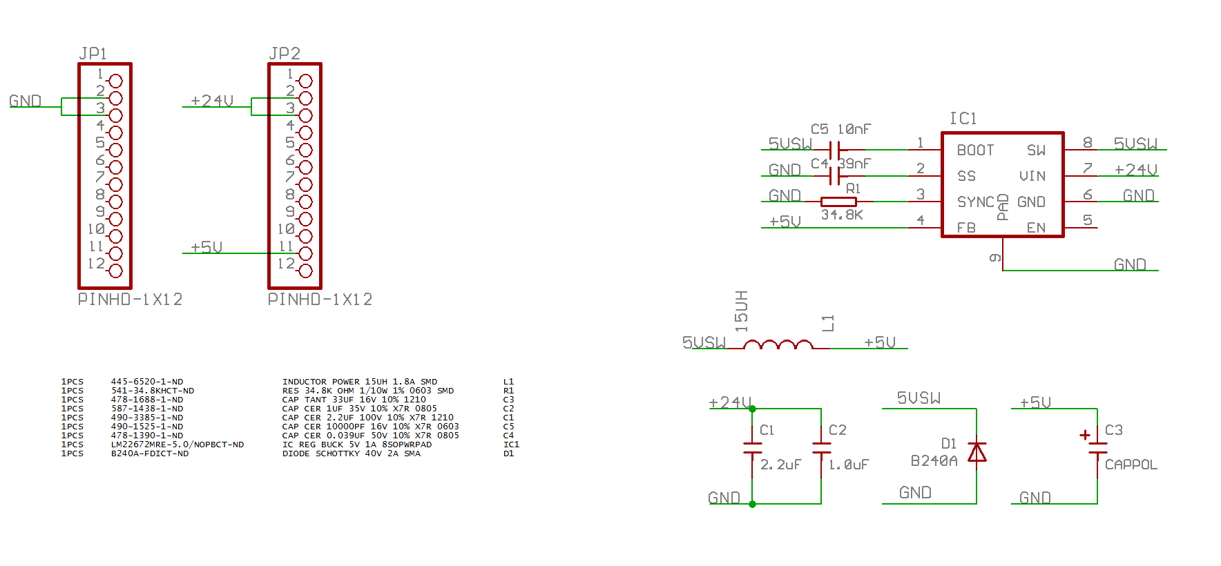
For our application we are utilizing small voltage regulator PCBs based on the LM22672 mounted onto a larger PCB (see attached picture). The input supply is 24VDC and the output voltage from the regulator is fixed at 5VDC. We have measured the load current to be approx. 350mA. 

The schematic for the voltage regulator PCB that uses the SWITCHER is attached. In addition to this, the main PCB on which this regulator is mounted has 470uF caps on the 24V and 5V sides, and a pair of TVS diodes on each side. 

During the process of bench testing our PCBs that use the regulator boards, we have so far encountered three regulators that have burned-out (released smoke from the SWITCHER). Also, when these regulators fail, the TVS diode on the 5V side gets damaged. All these regulators are from the same production run and whats confusing us is that not all the boards exhibit this behavior. We have attempted to stress test randomly picked boards and were unsuccessful in reproducing the failures. 

We would appreciate any kind of help or insight that you could provide towards resolving this issue.

Thanks.

  • Hello,

    I am looking at the image of the board you have posted. The layout on the switcher board is not optimized and that could be causing some really high voltage spikes on the input pin of the switcher. You could use a bandwidth unlimitted option on the scope and probe the Vin pin of the IC. You might see very large spikes on that pin. If those spikes can consistently stay over the abs max of the IC, it could damage the part. As an experiment, you can take a small 0805 0.1uF cap and place is right between pin 6 and 7 of the IC. Those are GND and VIN pins. This will help bypass any noise on the Vin pin and help quieten it.

    Ideally, you should have the input to the IC on the same side and it should not be going through a via. Vias add line inductance and cause noise. You also have relief connects at most of the places. The ground plane should be one copper pour and shouldn't be disconnected or have relief connects. Your Cin cap should sit flush on the ground plane. The SW node should be fat/wide and short. You have a thin trace running from SW to the diode and inductor. Please look at the image of the idea layout on page 18 of the datasheet. 

    I hope this helps.
    Regards,
    Akshay