Hello,
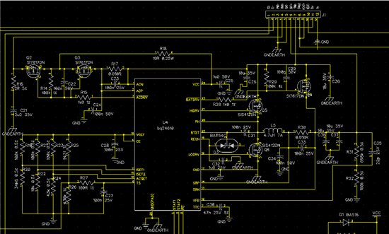
I've been wracking my brain and chasing my tail as to why my bq24610-based system is behaving this way. My circuit is virtually identical to the datasheet's 'Figure1', with values set for a 4-cell implementation as per the v1.5 excel calculations spreadsheet, with what I *think* is a fairly decent PCB layout. Schematic is attached:
My Problem:
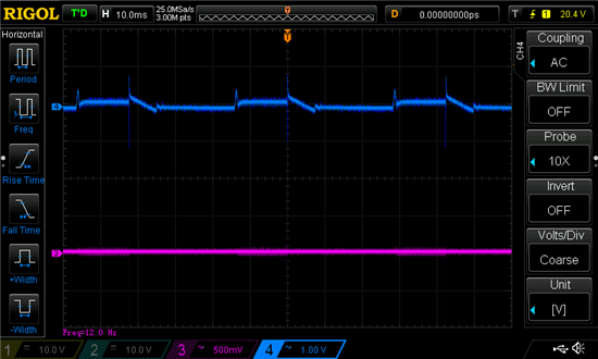
When the AC-adapter's DC input is applied & reaches the switch-over threshold (e.g. Vdc-in > Vbatt + ~1.0V), PG goes LOW solidly for 1 second. Then after 1-second STAT1 goes LOW (solidly), STAT2 remains HIGH, which indicates "Charge In Progress", but PG is oscillating at about 23Hz, and indeed the Gate drive to Q1/Q2 (ACFETs) & Q3 (BATFET) is oscillating (see attached pic). ("HIGH" & "LOW" here are w.r.t. pull-up resistors on these 3 status outputs, pulled-up to a 5V rail driven by a Vreg downstream from this bq circuit).
In the two scope shots below:
- (1) Yellow = Q4 FET gate (upper-buck)
- (2) Cyan = Q5 FET gate (lower-buck)
- (3) Magenta = Q1/Q2 ACFET gate
- (4) Blue = Q3 BATFET gate
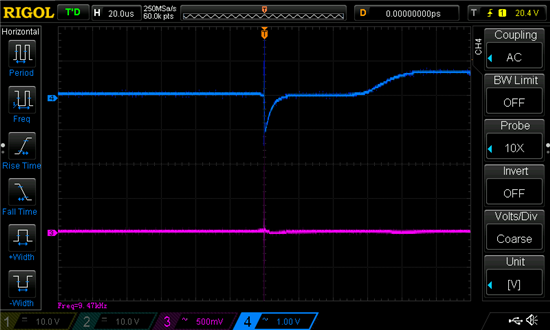
There is also 1 cycle of the Q4/Q5 buck-converter FETs turning on/off & back again (as far as I can tell only 1 cycle per 23Hz-oscillation period):
If I push the DC input V up high enough (>17V, but depends on the current-capability of my bench PSU), then my bench PSU will go into current-limiting at the same 23Hz. I have already killed one laptop-style 20V/5A PSU so far (the intended AC adapter for this system) with this treatment, although it turns out to have been a sub-standard Chinese cheapy. All testing is now being done with my max-3A & max-5A bench PSUs.
Notice also significant ringing on the gate voltage (10V/div).
What's more, with the Q4/Q5 buck FETs switching on for only 1 x 600kHz cycle throughout the whole period of the 23Hz oscillation of ACFET/BATFET, there is several amps flowing into my battery, even though the bq24610 isn't regulating voltage into it!
It's like there's punch-through happening between DCin & Vbatt - but I can't see how? I feel like I'm missing something completely obvious :-(.
I have the 100nF between gate & source of Q2/Q3 & Q4 supposedly to assist in the break-before-make timing built-in to bq24610.
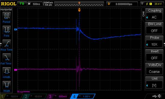
My Vref is good at 3.3V give/take a few mV, but both Vcc (4-Blue) & Vref (3-Magenta) have quite bad noise aligned with the ACFET & BATFET oscillation freq, which I guess it to be expected with what's happening. See a few captures of Vcc & Vref (AC-coupled) here:
Notes:
I notice there is a difference in the gate-drive arrangement of the datasheet (Figure 1), and the bq24610 EVM schematic. On the datasheet, the Q1 & Q2 ACFETs have BOTH gates driven through the single 1k resistor, but on the EVM schematic Q2 is driven via an extra 1k resistor, and the 100k/100nF pull-up is connected only to Q2's gate (not Q1 too), and an extra 100nF between Q2-gate & Q2-source. Can anyone explain these differences? The EVM's configuration is likely to result in near-instant switching of Q1, with much slower switching on Q2 (slower like what I'm seeing on both my Q1 *and* Q2).
I laid out my PCB fairly well, I think, carefully following the datasheet recommendations and their order of importance listed. I have 2 grounds, the 'power ground' and the 'signal ground', joined at only 1 point - the pin-25 heatsink pad underneath the bq24610, with a 4-layer PCB with one of the inner layers carrying the 2 grounds. Most of the circuitry (except for the programming resistors) takes up a space of only 30mm x 20mm.
My components are chosen almost exactly from the BoM recommendations in the datasheet.
The battery pack is a 4-series 2-parrallel arrangement of 18650 Li-Ion cells yielding 5200mAh capacity, with a Battery Protection Module based on the Seiko S-8254AAFFT chip, both supplied by Tenergy in California.
My client is expecting to purchase these bq24610 chips at a 1000/month rate once production ramps up starting in a couple of months, so I hope someone can help me with this!
Thanks, Anthony May. Sydney Australia.


