This thread has been locked.

If you have a related question, please click the "Ask a related question" button in the top right corner. The newly created question will be automatically linked to this question.

BQ34Z100 ROM mode and I2C timing documentation

Other Parts Discussed in Thread: EV2400, BQ34Z100EVM, BQ34Z100, BQEVSW

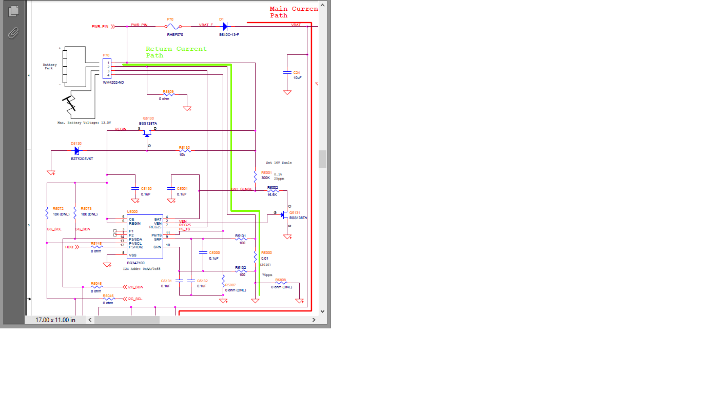
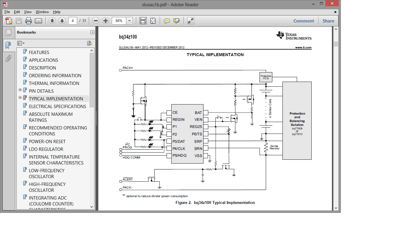
I am looking for real documentation (not just comments in a VB script) for ROM mode. It seems that ROM mode is largely undocumented - although slusau1b.pdf mentions BOOTROM mode, the command to enter ROM mode is not listed and no further references are provided.

I am also looking for documentation regarding I2C message timing - several forum posts indicate various delays between write and read portions of commands, delays between commands, and so on. The VB scripts also insert command-specific delays into the sequence.

Finally, I would like to set the I2C clock speed used in the EV2400.

Where are these things documented?

  • Further forum browsing indicates TI does NOT publish ROM mode register specifications.

    I have a working BQ34Z100EVM and EV2400 module. I have a proprietary board with an unconfigured BQ34Z100 chip. I am unable to drive the I2C on the proprietary board using the bq Evaluation Software due to communication timeouts.

    I have software that attempts to read and write the configuration based on the published subclass and block info in slusau1b.pdf. Although I can read individual blocks, I see occasional communication errors. I am unable to write a subclass block successfully.

    My best guess is that the default configuration AS SHIPPED is invalid, and that the BQ34Z100 on my proprietary board is somehow resetting. I am guessing at the reset because the subclass register appears to revert to 0x00 on its own. An internal reset would explain other symptoms (intermittent communications errors) that I am seeing.

    I cannot configure the BQ34Z100 via the eval software or via my own code (based on published documentation), and the ROM information is not published. It certainly seems as though I have wasted quite a lot of time trying to get this part to work. If there truly is no further information available that will allow me to configure this chip, please let me know so that I can start looking for an alternate part.

  • We have several documents available for download from the product website and the Going to Production (SLUA665) document is probably the one that you need. The device is shipped configured for 1-cell operation, so you will probably need to reconfigure it for a multi-cell pack. You will need to set the VOLTSEL bit in the Pack Configuration register, set the number of series cells and calibrate the voltage. This should clear up your problems with operation. Be sure the calibrate the device before sending the IT Enable command. If you still have communications problems, then check your I2C signals with an oscilloscope.

    The clock frequency on the EV2400 is fixed at about 90 KHz.

  • I cannot set the VOLTSEL bit because I cannot write the Pack Configuration register. The control status register reports 0x0000, so the device is not sealed. I don't think this is an I2C issue, but I would have liked to slow down the I2C clock just the same.

    I have already implemented the VB code in SLUA665. Why would the chip exit ROM mode when I tell it to erase the flash (write 0x0C to register 0x00, write 0x83 to register 0x04, write 0xDE to register 0x05, write 0x6D to register 0x64, write 0x01 to register 0x65)?

  • Can you use the bqEVSW to initialize the device to a good state by loading the default senc file into the flash? You can then setup the VOLTSEL and calibrate the device. I tried the erase DF commands and they erased the DF and did not place the device back into normal mode. Did you issue the checksum commands? if not, the device would have rejected the other commands that you sent. Try sending these after returning the device ot a good state.

    W: 16 00 0C
    W: 16 04 83
    W: 16 05 DE
    W: 16 64 6D
    W: 16 65 01

    bq34z100_R0_V0_06_BLD_0006.senc
  • I presume you mean the sequence indicated in SLUU904 in section 5.7.2 Reprogramming. I can send 0x000F to address 0x00, and the normal scan stops working at all (meaning it usually retrieves some but not all of the values). I select your .senc file and click "program", but I get error code 772 and the device is once again in gas gauge mode instead of ROM mode.

    I can, however, extract a .senc file without any problem, which is attached. 2161.bq34z100_Ruckstuhl.zip


  • I checked the senc file that you extracted from the device and it is exactly the same as the default senc file. What is you cell configuration? e.g.  3S2P, etc. ?? What type of cells are you using? Are you using the TI EVM?

  • I have no trouble with the BQ34Z100EVM in a 3S1P configuration with LiFePO4 cells. However, we want to integrate the chip instead of the module, and my understanding was that we would calibrate and run an optimization cycle for the proprietary board once we configured the BQ34Z100 on our board. 

    Unfortunately, I cannot configure the chip on the board. 

  • You should run the optimization cycle on your module to achieve the best accuracy. Can you use the bqEVSW with your module? If so, can you load a gg file into the device? Have you checked the I2C signal integrity with an oscilloscope?

    If you can send a schematic for the bq34z100 section of you module, then I can review it for problems that may affect performance.

  • When I use the bqEVSW with my board, the bqEVSW reports "No Acknowledge: VB_T2H_NACK" during the DataRAM scan, and leaves some fields empty (which is consistent with what I have seen with my software - I added repeats to my read commands so that I could work around this). The empty fields are consecutive but random.

    I cannot get a complete read of either the DataRAM or the DataFlash using the bqEVSW. I have no problem downloading the entire senc file using the same bqEVSW, however, so it is not an I2C problem.

    The I2C lines look clean on the oscilloscope. Am I correct to assume that the EV2400 pulls down the SCL line in order to try to reset I2C communications after errors?

    Is there a way to read internal temp while in ROM mode? The chip is reporting an internal temp of 38.5C (which sounds a bit high to me for a low-power part), and I would like to see if the internal temp drops while in ROM mode.

  • Does the bqEVSW auto-detect when you start it? Have you tried only selecting a couple of parameters are a time to see if the communications error are associated with a particular parameter? Have you tried more than one of your modules or more than one EV2400? You could also try an EV2300. its communication runs at about 60 Khz

    You cannot read the temperature when the device is in ROM mode.

  • I'm realizing that the SCL held low is probably clock stretching by the BQ34Z100. We did not measure the hold duration on the scope, but it was exceptionally long. How long is normal? The SCL line was not held low in ROM mode.

  • The bqEVSW usually autodetects when I start it. Occasionally I have to restart a couple times. I have tried to select a single parameter at a time and the bqEVSW refuses to write anything because it cannot preserve the original values of other data fields because it cannot complete a full read.

    I have tried this on both proprietary boards that we have. I only have one EV2400, so I have not tried a second one (or a 2300), but I have no problems talking to the BQ34Z100EVM and changing values via bqEVSW.

    The temperature appears to vary depending upon how frequently I try to scan the DataRAM with the bqEVSW.

  • The device will hold the SCL signal low when it is busy. It not hold it low for longer than 25ms on an SMBus interface, but it could be longer on an I2C interface.

    If you could send a schematic of your module, then I will review it for potential problems. You can send one of the modules to me and I can try to find the problem, if you want to do that.

  • The HDQ line is not intended for use at this stage and is connected to a High-Z input. The I2C lines have a 10K resistor listed as DNL (not populated) but are actually pulled up via a 1.5K elsewhere. Resistor R5808 in the lower right corner is also listed as DNL and is not populated 


  • You will probably find that 1.5 kohm pull-up resistors are too small and the I2C signals are not pulling low enough for reliable operation. We recommend using 10 kohm resistors. Please try using pull-up resistors that are larger than 5 kohm.

  • I agree that 1.5K pullups is on the small side, and the hardware engineers are changing that. But that doesn't exactly explain why an erase command would exit ROM mode instead of being ignored. I don't think this is an I2C problem.

  • I misspoke - the hardware guys were questioning the serial resistors on the I2C lines - your EVM has 200ohm, while our board does not. Can I assume that the serial resistance is unnecessary?

    Your recommended 10K pullups will affect our maximum I2C clock rate, which drove the selection of 1.5K. How can we approach your stated 400KHz maximum clock rate if we use 10K pullups?

    I am still unconvinced this is an I2C problem. I still do not see how I can download the senc repeatedly without problems but cannot erase the data flash. I have asked that the hardware guys try 5K pullups in spite of this. Is there anything else you can suggest in the meantime?


  • The series resistors are used for ESD protection and they are not necessary for I2C communication. You will probably have to look at the I2C waveforms to size the pull-up resistors, but I think that it would be good to get communications to work properly before trying to maximize the clock frequency.

  • replaced 1.5K pullups with 5K - no change.

    We put REG25 on the scope for kicks - it's bouncing 0.1v - from 2.4v to 2.5v or so, and noisy. At highest time resolution we have (10ns), it looks like we're getting a pretty fast digital signal. Grabbed some video via Android phone and attached it (my apologies for the poor focus). Isn't REG25 supposed to be stable?

  • You are correct that REG25 should not pulse as shown in the video and I did not see any issues with the schematic. Do you think that noise could be induced onto REG25 from your external thermistor? If you would like to send a pack to me, then I will try to find the source of the noise.

  • The external thermistor was not connected. Also, the REG25 output was quite stable in ROM mode, so it is unlikely to be external interference.

    Is there something I can try here (short of replacing the chip) that would definitively indicate a bad chip?

  • The pulsing seemed to occur at about a 1 second rate and this is the rate at which the device updates parameters. The device will draw more current at this time. I would check the REGIN signal to see if it is stable. If it is pulsing, then check on the battery side of your regulator. If you do not see any pulsing on REGIN, then check other signals around the device for noise. the firmware is not running in ROM mode, so this would explain the difference that you see when in ROM mode.

  • We see a similar pulsing (around 0.15v-0.2v, same period, less noise, not in ROM mode) on REGIN. REGIN is normally about 4.5v. The battery side of our regulator is stable. The gate side is stable as well.  

    I was expecting REGIN to vary a little depending upon current consumption, and the voltage did not drop enough for me to worry about starving the chip for current. I had thought that as long as the REGIN voltage doesn't drop below 3V or so, then we should be OK.  

    Please note that the REG25 noise showed up with a 1s regularity, but had a significant high-frequency component that is also not present in ROM mode. Does that match the internal clock frequency to the internal flash?


  • Maybe the REGIN regulator is weak. You could try powering REGIN with a power supply to see if this make a difference. The device runs at about 2 MHz internally.

  • we bypassed Q5130 (the voltage-limiting transistor) and fed CE and REGIN from the output of a 3V regulator we had elsewhere on the board. REGIN is now stable, but REG25 still shows the same noise.

    What is the frequency and duty cycle of the Ven output? It doesn't look like what I expected, and in fact looks like the same frequency as the extra noise on the REG25 line.

  • VEN will pulse high for 125ms every 1s when in normal mode and every 20s when in sleep mode.

  • We're seeing something that is not a 1s periodic pulse. We saw a 10ns period squarewave with a 99% duty cycle. I didn't record whether the output went all the way down to 0, so I'm emailing the hardware guy who was looking at the scope with me. But we saw something that is definitely not 1Hz.  

  • I am not aware of anything on the device that would cause that waveform. I can look at it on the bench, if you wan to send a pack to TI.

  • Apparently we are supposed to have a 1uF capacitor between REG25 and Vss.

    This is missing from your reference diagram for the BQ34Z100.

    Can you confirm that the missing cap can cause spontaneous resets of your chip? For the past month we have been trying to figure out what appears to be a chip reset during internal flash write/erase.

  • We have a 1uF capacitor between REG25 and VSS in the reference design. This clip is from the schematic in the datasheet and EVM User's Guide.

  • Correction - it is missing from the "typical implementation" diagram in Figure 2. It is present in the application schematics. There is also text in the electrical specs indicating 1uF across LDO25, which is presumably REG25.

    Can you confirm that the missing capacitor can cause spontaneous resets?


  • I can confirm that the BQ34Z100 resets on flash write without the 1uF capacitor between REG25 and VSS. This capacitor is missing from the Typical Implementation diagram in Figure 2 of slusau1b.pdf.

    Perhaps TI could fix the documentation? The external capacitor is required for operation, but is not listed in the Typical Implementation. The need for the capacitor is not obvious - even the experts at TI missed it when reviewing my schematic last month.

    Credit for the solution goes to Jason Gin, whose post about a different chip hinted at the problem with my board. Wish I could mark his post as the answer.

    http://e2e.ti.com/support/power_management/battery_management/f/180/p/308135/1072433.aspx#1072433

  • The 1uF capacitor is required. The Typical Implementation diagram in Figure 2 is not a detailed schematic. There are other external components missing from it as well. You should refer to the Application Schematics as a detailed reference.