This thread has been locked.

If you have a related question, please click the "Ask a related question" button in the top right corner. The newly created question will be automatically linked to this question.

TPS54020 failure (internal lower side FET short circuit)

Hello everyone.

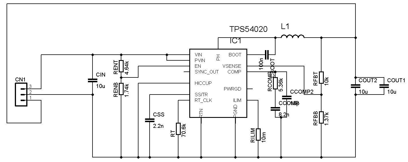
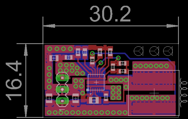
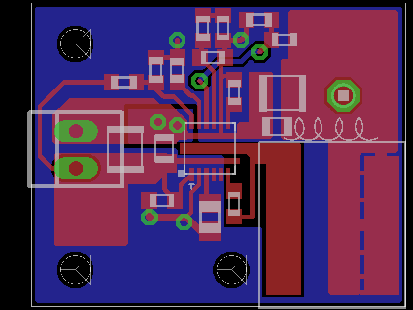
I made a small 15V to 5V  (7A out) step down converter according to webench:

7713.webench_design_3562831_6_903630554.pdf

Upon turning the power on (15V, output floating), the device immediately gets hot.

Current goes to more than 1 A (stil open circuit) immediately.

I made a second board, with a different chip, this time it did not get hot, current was few mA (good), but...

Neither gave me any output.

Two separate boards and separate devices, in both I measure short circuit on the lower side transistor.

I bought extra device to test again. I started with a small voltage and at about 4.5V inut the current suddenly jumps to 0.5A and increases to more than 1A at >6V. I stayed on 4.5V and connected a light bulb which lit up dimly (the output voltage was 0.5V). As I increased the voltage to about 9V the bulb was erratically getting brighter and dimmer and I could hear the switching noise. The input current was about 1.5A and then the chip failed.

This is now the 3rd chip that failed. I checked all component values on the PCBs and they are all as per the schematics.

No component is further than 6mm from the chip.

The boot voltage was correct (I do not remember it now, though).

Any help as for why the chips are failing would be deeply appreciated.

Wojciech

  • Wojciech,

    The schematic you posted is the Webench report. Can you post your actual schematic? What PWB are you using? Can you also post your actual BOM with part numbers?

    Regards,

    MC.

  • Hi, thank you for reply.

    I have extra capacitance attached parallel with the load, totalling 67uF.

    this is the actual parts I ordered:

    ID

    Description

    Mftr. & Part No.

    IC1

    BUCK, 4.5-17V, 10A, 1.2MHZ, ADJ, 15VQFN

    TEXAS INSTRUMENTS - TPS54020RUWT

    CIN, COUT

    CAP, MLCC, X5R, 10UF, 25V, 0805

    AVX - 08053D106KAT2A

    L1

    INDUCTOR, PWR, 3.3UH, 25A, 20%,21MHZ

    COILCRAFT - XAL1010-332MEB

    CBOOT

    CAP, MLCC, X5R, 100NF, 50V, 0603

    TDK - C1608X5R1H104K080AA

    CCOMP1

    CAP, MLCC, C0G/NP0, 8.2NF, 25V, 0603

    KEMET - C0603C822J3GACTU

    CCOMP2

    CAP, MLCC, C0G/NP0, 18PF, 50V, 0603

    KEMET - C0603C180J5GACTU

    CSS

    CAP, MLCC, X7R, 2.2NF, 100V, 0603

    AVX - 06031C222KAT2A

    RCOMP

    RESISTOR, 0603, 5K36, 1%

    VISHAY DRALORIC - CRCW06035K36FKEA

    RENB

    RESISTOR, 0603, 1K74, 1%

    VISHAY DRALORIC - CRCW06031K74FKEA

    RENT

    RESISTOR, 0603, 4K64, 1%

    VISHAY DRALORIC - CRCW06034K64FKEA

    RFBB

    RESISTOR, 0603, 1K37, 1%

    VISHAY DRALORIC - CRCW06031K37FKEA

    RFBT

    RESISTOR, 10K, 0.1W, 1%, 0603, SMD

    VISHAY DRALORIC - CRCW060310K0FKEA

    RILIM

    RESISTOR, CURRENT SENSE, 0.01 OHM, 0.5W

    BOURNS - CRF0805-FX-R010ELF

    RT 

    RESISTOR, 0603, 0.17W, 143K, 0.1%, 25PPM

    TE CONNECTIVITY - RP73PF1J143KBTDF

    RT 

    RESISTOR, 0603, 0.17W, 140K, 0.1%, 25PPM

    TE CONNECTIVITY - RP73PF1J140KBTDF

    The two RT resistors are placed in parallel, as I could not find a value that was required after the report was generated. This is the PCB layout:

    It is a standard 1oz 1.6mm FR4. with 0.6mm vias. Dimensions in mm.

    Sorry, the layout has all the names deleted because it is too small.

  • Wojciech,

    I don't see any big issues with the schematic, but there are issues with the layout. As you mention there are no RefDes's on the layout picture, but I think your 10uF input cap is located at the very north west corner of your PWB as pictured. Is that correct? If so, that will definitely cause issues. The input cap should be butted right up against the device, placed as close to the device as your manufacturing rules allow. The cap should be right up against the outer two strips of the HotRod package. It must also be on the same side of the board as the device and not connected through vias. Vias will add far too much inductance and resistance. The di/dt between the input cap and the device is extreme, so this connection must be done well.

    Can you take a scope shot of the waveform at PH to PGND and PVIN to PGND during operation? That might provide some important information.

    There are also other issues with the layout. If you are interested you can provide your email address and I can contact you off line.

    Regards,

    MC.

  • You are right about the location of the CIN,

    Does that mean I might have too large ripple into the device (and EM noise) and possibly oscillations?

    I will adhere to the suggestion and post here the result as soon as possible (I am not in the lab currently).

    Unfortunately I can't get access to the oscilloscope until after Monday, only then could I post pictures.

    I am very interested to learn more about layout, here is my email: wojtek(.)marcinek(@)gmail(.)com

    Thank you,

    Wojciech

  • Hello everybody.

    I have redesigned the voltage regulator from start. I moved the capacitors close to the chip and got rid of all the vias in the hight current loops (which were made smaller).

    The new layout looks like this:

    This layout works very well, I am getting desired output voltage and the power consumption is about 10mA at 15V when open circuit.

    I should also mention I did the PCB at home with toner transfer, I have no solder resist and the board sill works!

    I soldered it with solder paste and bathed in isopropyl alcohol to dissolve all the remaining flux/rosin/stuff.

    For all those who have similar problem, if the layout is closer to what I had in the beginning, I suggest to change it. If the layout is closer to my final, unfortunately I do not know what might actually be the problem.

    Wojciech