This thread has been locked.

If you have a related question, please click the "Ask a related question" button in the top right corner. The newly created question will be automatically linked to this question.

TPS63030 Distortion in Transition Zone

Other Parts Discussed in Thread: TPS63030, TPS62730, TPS62740

Can someone tell me if this is normal behavior?

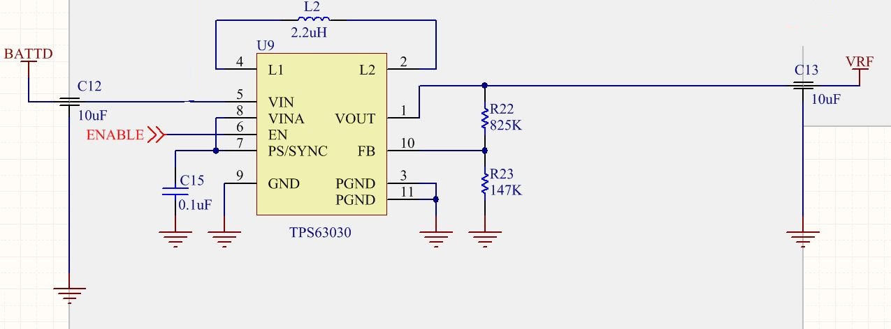
I am using a TPS63030 to generate 1.9V from a 1.8V - 3.2V (2 AA alkalines) supply.  Here is my circuit:

The layout is very well done, with solid ground connections, a ground plane under the circuitry, a solid ground connection to the power pad, very short traces, and the entire layout area is ~0.3" x 0.3".

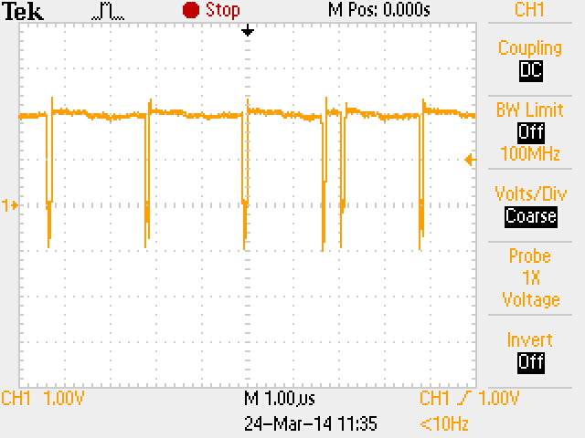
The TPS63030 operates in BUCK MODE with Vin between 3.2V and 2.6V.  Here are the switching waveform and the output ripple at 2.6V 62mA in, 1.9V out:

The TPS63030 operates in BOOST MODE with Vin between 2.1V and 1.8V (UVLO point).  Here are the switching waveform and the output ripple at 2.1V 97mA in, 1.9V out:

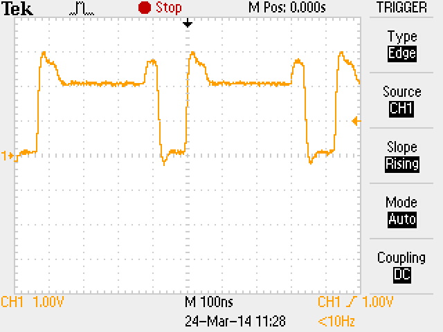
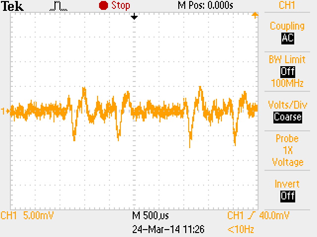
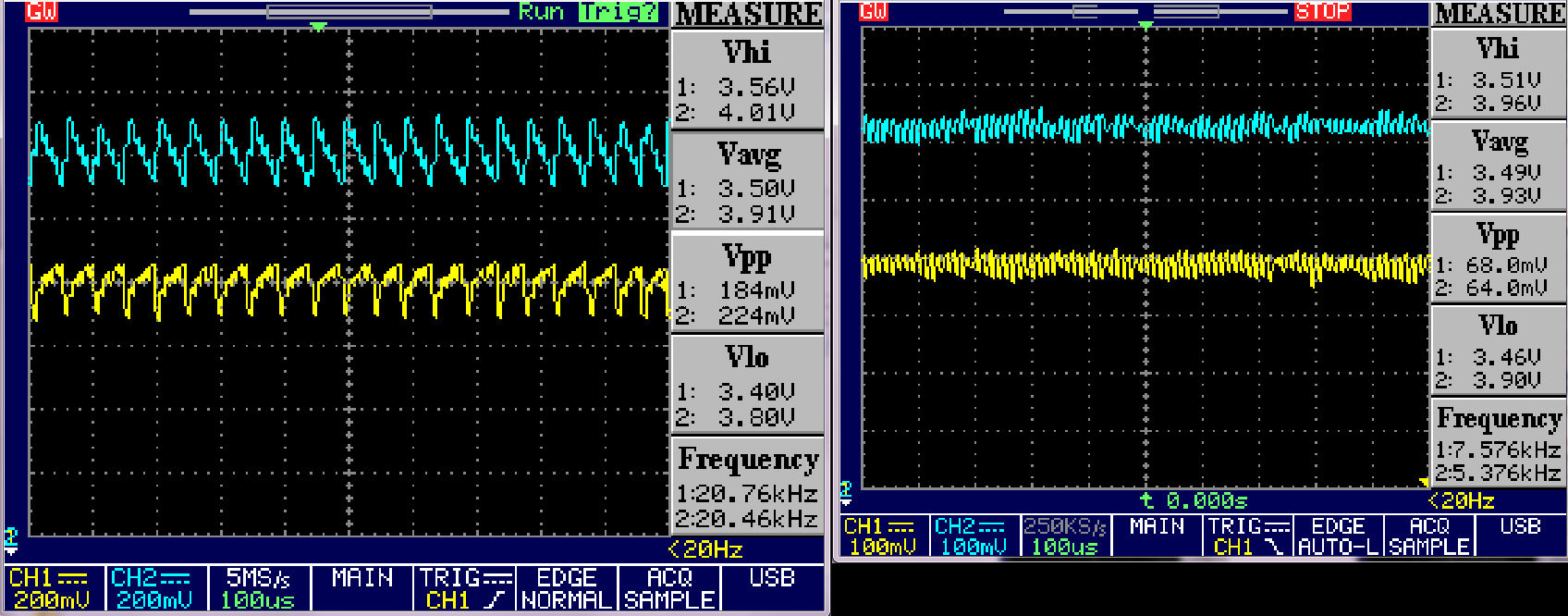
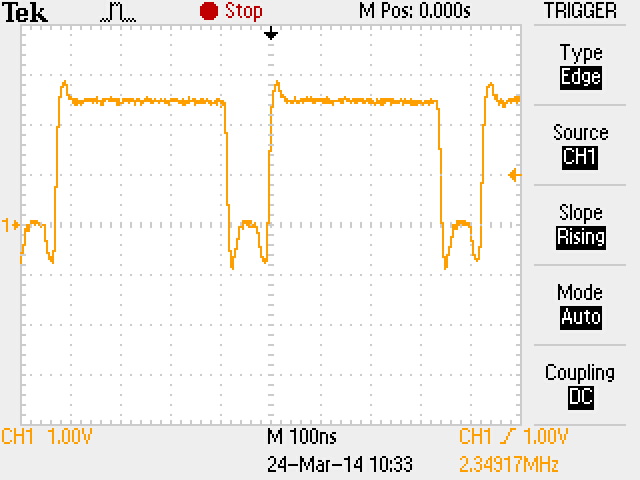
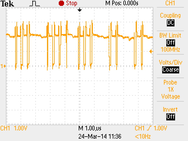
The TPS63030 operates in MIXED MODE with Vin between 2.6V and 2.1V.  Here are the switching waveforms (each side of inductor) and the output ripple at 2.3V 87mA in, 1.9V out:

"BUCK" side

"BOOST" side:

Output ripple:

The increased noise level and the varying nature of the BUCK-to-BOOST transitions is creating speaker noise in the audio circuit that is powered by this converter.

Is this something that I will just have to filter out, or is there some way of adjusting the circuit to eliminate this excess noise in the BUCK-to-BOOST transition zone?

Thanks in Advance,

Ed

  • More input and/or output capacitance will likely improve things a lot.  You need to make sure that the input voltage is holding steady, even with whatever source impedance (from long wires or the battery) you have.  A 100uF or so ceramic on the input should help this.

    More output capacitance is usually desired for these devices, so you might try a 22uF or two in addition.

    Finally, if your currents are that low (<100 mA), a buck only solution might give you more run time due to the lower Iq.  TPS62730 and TPS62740 are good devices to look at.

  • Well, added two 47uF caps in parallel to both the input and output sides.....no change.

    I was pretty sure this wasn't the problem, since the noise only appears when the converter is switching toggling between BUCK and BOOST mode.

    Perhaps the inductor choice?  Could some inductors behave strange when switching between BUCK and BOOST mode so quickly and often?

  • Were you able to look at the input voltage and verify it's steady?

    Yes, the noise will be higher in buck/boost mode.  Adjusting the inductor value may affect it.  You could try 1.5uH and 3.3uH and see if either help it.  The goal here is to find an application solution that gets the noise low enough for your load.

    Also, are you testing with an electronic load or your real system load?

  • Yes, the input voltage is steady.  Yes, I am testing with my real system load.

    I found something interesting.  I use another TPS63030 circuit to generate a 3.3V output on the same PCBA.  It has the same layout and components (except the voltage-divider resistor values) as the 1.9V circuit that is giving me trouble.  Here is the schematic:

    When I viewed the output noise on this circuit, it was <5mVp-p regardless if the TPS63030 was in BUCK mode, BOOST mode, or MIXED mode.  The scope showed a very small increase in output noise when in MIXED mode, but it was negligible and showed no signs of instability.  In addition, the transition from BUCK to BOOST was only about 50mV wide, versus the 500mV width of the 1.9V converter.

    I changed the resistor divider to re-program this 3.3V converter to 1.9V output and added a resistive load of about 75mA to match the usage environment of the original converter that is giving me trouble.  This converter now exhibits the same instability as the original converter.

    I also changed each of the voltage-divider resistors to 10% of their original values to reduce noise coupling into the FB pin.  This had no effect.

    The problem seems to be an instability in the circuit when programmed to operate at 1.9V and operated with an input voltage that causes the TPS63030 to operate in MIXED mode.  When operating in BUCK or BOOST mode only, the switcher works perfectly.

    I am planning to try different inductor values and inductor types, but I have no data to support why this might change anything.

    Does this generate any new ideas?

    Regards,

    Ed


  • You might try a feedforward cap across the high side FB resistor.  Something in the range of 10-100 pF should help by sending some of the output signal to the FB pin quicker.

    A low Iq buck like TPS62740 is still possibly an overall longer battery life solution.

  • I've just had the same experience with my implementation of the TPS63030 boosting 3.3-4.5 volts to 4.0v. I was getting 177mVpp on the output! I tried 94uF caps on the output and 47uF on the input side. that make the waveform look like a triangle wave..  /\/\/\/\/\/\/\\/\ instead of |\|\|\|\|\

    my divider network is 1.24M / 178k and I now have tested a 33pF cap across the 1.24M resistor.

    Before the modification to 47uF output caps and 33pF feedback bypass caps the voltage drop across the OR arrangement looked like;

    <10mA to 120mA pulses.. yay..

    10-90mA draws alot smoother over the input diodes

    Resulting in a nice output voltage ripple change from 200mVpp to 64mVpp

    I haven't yet experimented with the device at maximum load or with larger bypass capacitors. That's a job for later.. But you get the idea... the bypass capacitor option should be mentioned in the spec sheet ?? or a tech note??

  • Check out the drop in input ripple (caused by diodes) and output ripple helped by the bypass cap across R134.