


Hi,
We are using BQ77910 for Protection in one of our projects.
My main query is related to programming/writing the data to EEPROM from the microcontroller.
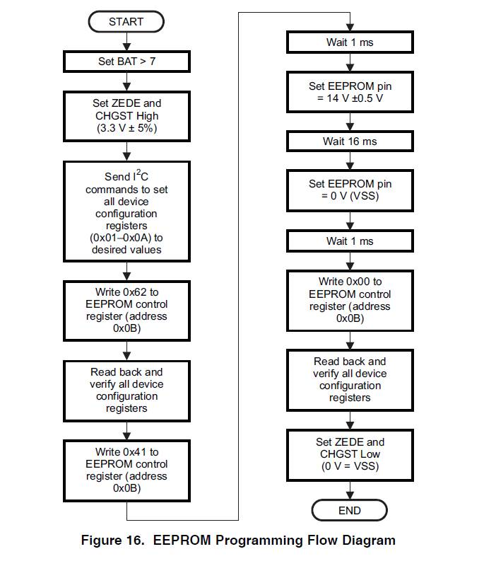
I followed this flowchart and wrote the code exactly as the flowchart below.
In the below Flowchart, We are reading the data registers for verification 2 times, When i read for the first time i am getting all 10 Bytes of data (with only FIRST Byte missing).
in the second Verification (reading data) I get all random data.
If i reset and read the data, its all 0xFF
The following is the code i am using:
int main(void)
{
	unsigned char UC_NumberOfCells = 0;

    SysCtlClockSet(SYSCTL_SYSDIV_1 | SYSCTL_USE_OSC | SYSCTL_OSC_MAIN | SYSCTL_XTAL_8MHZ);

    // ------------------------------------------------------------------------------------- Fz_Debug
#ifdef DEBUG_MODE
    //ucDCard = MODBUS_DCARD_M; // for testing ModBus
    ucDCard = I2C_DCARD_M;    // for testing I2c
    //ucDCard = UART_DCARD_M;    // for testing UART
#endif // End of Debug Mode
    // ------------------------------------------------------------------------------------- Fz_Debug

    // Initialises the Communication Protocols
    Init_Cards();

    ChangeSOCI2CSpeed(50000); // 50KHz - SOCI2C

    //-------------------------------------BQ77910 Testing--------------------------------------
    char i, BQtest[10] = {0},BQtest2[10] = {0};

    // CHGST and ZEDE Pins on the BQ77910 Need to be HIGH to Write/Read from the IC

	// Enable Ports
	SysCtlPeripheralEnable(SYSCTL_PERIPH_GPIOB);
	GPIOPinTypeGPIOOutput(GPIO_PORTB_BASE, GPIO_PIN_5 ); // Configure CHGST PIN as O/P

	SysCtlPeripheralEnable(SYSCTL_PERIPH_GPIOE);
	GPIOPinTypeGPIOOutput(GPIO_PORTE_BASE,GPIO_PIN_3 ); // Configure ZEDE_EN PIN as O/P

	SysCtlPeripheralEnable(SYSCTL_PERIPH_GPIOA);
	GPIOPinTypeGPIOOutput(GPIO_PORTA_BASE, EEPROM_W_EN ); // Configure EEPROM_W_EN PIN as O/P

	//Set ZEDE and 	CHGST High	(3.3 V ± 5%)
	CHGST_ENABLE_M; // Enable  CHGST PIN
	ZEDE_ENABLE_M; // ENABLE ZEDE_EN

    while (1)
    {
        for (i = 1; i < 0x0B; i++) // Fz !Fz_Mod : z starts from 1
        {
        	//Send I2C commands to set all device configuration registers (0x01–0x0A) to desired values
            Write_SOCI2C_Byte(BQ77910A_ADDRESS, i, bq77910a_data[i-1]); // Fz

            //Wait 10mS
            Delay_ms(10); // Fz
        }

    	// Write 0x62 to EEPROM control register (address 0x0B)
    	Write_SOCI2C_Byte(BQ77910A_ADDRESS, 0x0B,0x62);

    	Delay_ms(10);

    	// Read back and verify all device configuration registers
    	for (i = 1; i < 0x0B; i++)
		{
    		BQtest[i - 1] = Read_SOCI2C_Byte(BQ77910A_ADDRESS, i);

			Delay_ms(10);
		}

    	// Write 0x41 to EEPROM control register (address 0x0B)
    	Write_SOCI2C_Byte(BQ77910A_ADDRESS, 0x0B,0x41);

    	//Wait 1 ms
    	Delay_ms(1);

    	//Set EEPROM pin HIGH
    	EEPROM_W_ENABLE_M;

    	//Wait 16 ms
    	Delay_ms(16);

    	//Set EEPROM pin HIGH
    	EEPROM_W_DISABLE_M;

    	//Wait 1 ms
    	Delay_ms(1);

    	//Write 0x00 to EEPROM control register (address 0x0B)
    	Write_SOCI2C_Byte(BQ77910A_ADDRESS, 0x0B,0x00);

    	// Read back and verify all device configuration registers
    	for (i = 1; i < 0x0B; i++)
		{
    		BQtest2[i - 1] = Read_SOCI2C_Byte(BQ77910A_ADDRESS, i);

			Delay_ms(10);
		}

    	//Set ZEDE and 	CHGST LOW
    	CHGST_DISABLE_M; 	// Disable  CHGST PIN
    	ZEDE_DISABLE_M; 	// Disable ZEDE_EN
    }
}
