This thread has been locked.

If you have a related question, please click the "Ask a related question" button in the top right corner. The newly created question will be automatically linked to this question.

LM2676S load response failure

Other Parts Discussed in Thread: LM2676, LM22676

Hello,

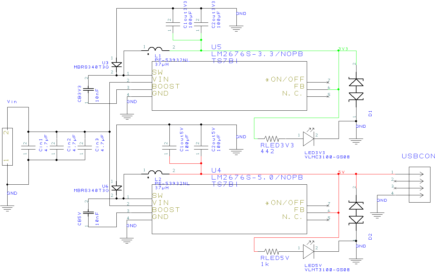
I'm using the LM2676S-5.0 and 3.3 on the same PCB, using the same input voltage. Both are working fine and the 5.0 is powering the Raspberry Pi just fine. I designed the 5V for 2A and the 3V3 for 1.5A with an input voltage of 8-40V using the steps said in the datasheet. This resulted in the following schematic:

And the PCB design:

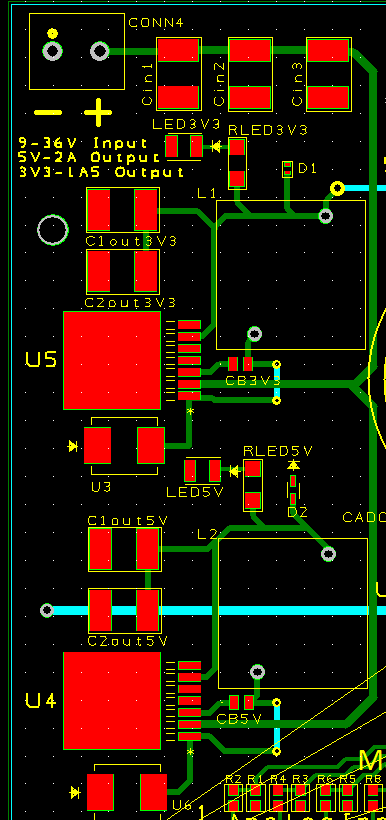
Where the top layer is poured GND.

However, today I went to test the load response using an measured 3.3ohm power resistor and the following happened:

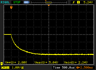
The voltage just crashed.. The 3V3 is responding okay but when changing to a 2 ohms resistor it also failed to maintain a proper voltage.


The components used are the following:

Cin = 3x T495D475K050ATE300
Cout = 2x2 TPSD107K010R0100
Diode = 2x1 MBRS340T3G
Inductor = 2x1 PE-53932NL

The only recommendation I didn't really follow was placing the Cin's as close as possible to the LM2676, also it recommended 2x input capacitors for the 3V3 and 3x for the 5V. However, as this is just used to reduce fluctuations on the input I can't see how it would be so destructive for the higher loads. The power supply used for Vin is a 24V/5A Siemens SITOP.

What can I do/change to stop the voltage from crashing down and why is it powering my RPi just fine, while that also draws 700~1A?


Thanks for the advice!

  • Hi Falco,

    Question 1:  Are you applying the load resistor while the Razberry PI is powered.  This would add the load currents together and you might hit the current limit.


    2) With your Vin caps far from Pin 2 and the Anode of the recirculating diode you are adding a lot of ground bounce to the circuit.  This might be causeing the part to falsely hit current limit early.  Try Addin a capacitor close to pin 2 and the gorund of the diode to lower noise


    3) Your power traces are long and thin.  Each square is 0.5 mOhms for 1 oz copper.  You have hundreds of squares in the traces I see.  this would be several hundreds of mohms and while this wouldn't cause the issue you are seeing it isn't good practice because of the large voltage drops.


    Regards,

    Marc


  • Hi Marc,

    Thanks for your reply! No, while testing with the load resistor the Raspberry Pi was not connected, just the bare board.

    About 2), I hope that moving the Vin caps will solve the problem, and I guess adding the omitted Vin caps will hopefully solve some problems too. Also, 5/3,1=1,6A is pretty far from the limit, or can this really cause that big kind of spikes? And when it 'crashes' to 2,2V the current it draws is a measured ~0,7A, shouldn't it just recover back to 5V then?

    By squares I think you mean the grid? That isn't a static factor, since I can change the grid size.. Anyways, the Vin trace is 0,9mm wide, all the traces related to the LM2676 are 0,6mm and all other signal traces 0,4mm. I'm not sure about what planes to use though. On my current PCB only the top layer is a ground layer, the bottom is unused. But because I have 2 voltages (3,3V and 5V) I don't know which one to make a plane. Or could I make 2 planes since the 5V pretty much only needs to go to an USB connector and a voltage reference chip? Or even 3 planes, making the 3V3 and 5V plane more like a really wide trace surrounded by ground? It is a 2-layer PCB.


    With kind regards,

    Falco

    Edit:

    Would this be a better PCB design?

  • Counting squares is just a way to estimate the resistance of a trace.

    The bottom line is that your traces, in the power paths, are much too thin. 

    You can use planes or just much wider traces to connect the inductor, diode, and input capacitor.

    Once the device goes into current limit, it requires a much smaller load to come out again.

    FD

  • Uh, maybe I'm missing the point of what you are trying to tell, but the inbuilt trace width calculator in Designspark PCB says that with a trace thickness of 70µm, ambient temp 20 degrees celcius and an allowable temperature rise of 10 degrees a trace width of 0,4mm would already suffice for the maximum load of 2A..

    Also, I can't really fit any wider traces to the pins right? 1mm really is the max then.. And when using planes, is it okay for it to also be underneath the inductor taking EMI into account? Or should that be a ground plane then?

    Edit: ah, after googling the counting squares method I realize what you mean. So that's a yes for using planes for both 5V and 3V3 on the bottom layer next to each other I guess.

  • The maximum temperature rise of the trace is a minor concern with a switcher, since the traces must be much larger to reduce the resistance and/or inductance.  The voltages and currents in a switcher have very fast edges and large peaks.  Therefore, resistance and inductance is the limiting factor. 

    The following app notes are good references : SNVA021C, SNVA054C, SLUP230

    Also, please look at the layout example in the LM22676 data sheet.

    FD