This thread has been locked.

If you have a related question, please click the "Ask a related question" button in the top right corner. The newly created question will be automatically linked to this question.

TPS43060 over dissipation: vcc R question

Other Parts Discussed in Thread: TPS43060EVM-199, TPS43060

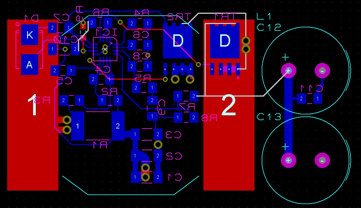
We are using the 43060 in a 12V to 50V 0.8A boost circuit.  Switching frequency is about 300kHz which we are using with Infineon BSC340N8 low gate charge FETs.  The chip gets very warm and eventually fails in the corner of the package close to the VCC supply.  It seems that the VCC supply is overloaded and doesn't appear to have any form of protection.

We have added the 2R resistor recommended (on the last line of the data sheet almost as an afterthought) although there's no information about how the value should be selected.  The resistor is also shown between the chip and the output cap: is that right?

Should we be increasing the value of the resistor to limit current into the boost diode?  If so, by how much?

  • Hi Rob,

    The 2R resistor is the recommended value for all conditions. I'm not so sure if the VCC supply is overloaded but you could check by measuring the resistance of the pins near it to PGND. It may be one of the other circuits near it as all of the pins for the internal gate drivers are in this area.

    Did you observe any other unexpected behavior other than the IC heating up? Such as a lot of jitter in the SW node.

    I'd also like to check a few more details on your board. Could you share the full part number of the MOSFETs?Was this on a EVM or a custom board? If it's a custom board can you share the schematic and layout?

    Best Regards,
    Anthony

  • I was a bit unsure about the position of the 2R: should it be isolating the output cap from the device?  Are there no stability issues?

    We didn't look at the SW signal to see any jitter although the output voltage varied a bit.

    Full MOSFET pn is BSC340N08NS3.  They were recommended by Webbench.  It's a custom board, the circuit is attached as is the layout.  There's a problem with the layout in that it was designed with the rectifier FET (TR1) the wrong way round so some cutting and re-wiring was necessary, shown in grey.   The 2R resistor has also been added. There is a single ground plane beneath all the components, not shown for clarity

    5383.50Vsupply.pdf

  • Thanks Rob. The schematic looks good. I can't see the layout very clearly though. Could you post a bigger image?

  • Yeah, bmp format isn't great but our CAD system can't export in many formats.  Try this one, generated from a screenshot.  Once again the grey lines are links added to correct errors.

    Thanks for your help in this.

  • Hi Rob,

    Thanks for the new image.

    I'm not so confident in this layout and it could definitely be a source of your troubles. I've listed a few specific things I noticed below.

    Some of the signals in the power path have quite small connections. I cannot see where the drain of the low-side FET is connected to the source of the  high-side FET. Is it just this grey wire connection? Same comment on the output voltage connection of the output capacitors to the high-side FET drain.

    R8 and C9 return to GND goes to the input capacitors which is more of  PGND area. These should return to AGND first. Also the placement of a lot of the 0603 R's and C's is not very ideal. Specifically pay attention to the GND pin they return to first.

    I'd recommend copying the TPS43060EVM-199 placement and routing of the small R's and C's as close as possible here. I think you could copy this placement without too much trouble on your board then place the power stage (input caps, inductor, sense resistors, FETs and output caps) where you need them to be for your board shape. It looks like you were able to get all of this on one side and put the inductor on the other.

    For the power stage it's important to minimize the length of connections and use wider traces as they carry higher currents and can cause noise. For the analog control circuitry its important to keep these away from the power stage components current paths and return them to the AGND pin.

    Best Regards,
    Anthony

  • I'm getting a bit twitchy about the TPS43060 if it's this sensitive to layout.  The layout isn't perfect I freely admit but surely not so bad as to cause immediate death of the device.  In any case after consideration asking it to produce a 50V output is a bit too close to its limits: HDRV is only a spike away from its abs max rating.

    Should the device work OK with a diode instead of the high side FET?  I know efficiency is lower but with a 50V output this isn't such an issue.  We are seeing the device working in DCM all the time so the inductor current doesn't reach 1A and the output voltage droops with any significant load.  Ft has been reduced to ~100kHz and the inductor increased to 100uH btw

  • Switching power supplies in general are sensitive to layout due to the nature of what they are. They incorporate both a high frequency switching currents and voltages with sensitive analog control circuits. Layout can cause IC failure if it causes the supply to be unstable leading to unusual stress above the absolute maximum ratings of the IC.

    I wouldn't be too worried about 50V output. There are generally not any spikes on the HDRV signal because the gate of the FET usually has enough capacitance to clamp any overshoot. But the device would work as a non synchronous converter. I would not expect the output voltage to droop with significant load though. You may want to check if the switching waveform looks stable as the load is increased.

  • The switching waveform is beautifully stable; just not the right duty.  With a 330R load it settles at about 40%, way less than the ~70% calculations say it should.  Output voltage droops from 50 to about 30V. The inductor current barely reaches 1A and decays to zero during the low side off time.  I would expect an inductor current  around 4A peak and the chip to work in CCM.

  • It may be reaching current limit sooner than expected due to noise. Since the switching is stable then there shouldn't be any issues with the loop. Also with the 10mOhm sense resistor at 1A peak current the sensed voltage should be only 10mV. To see if the device is being current limited, the COMP voltage can be measured. If it is at the 2.1V maximum clamp voltage then the device is operating in current limit.

  • The COMP voltage rises from about 1 to 1.4V with a 330R load, so nowhere near the 2.1V suggesting current limit.  The duty appears to settle to the value allowing the inductor current to fall to zero at the end of the cycle.  The device does not seem to want to enter CCM.  I notice that you advised someone else on the forum to unbalance the resistors in the current sense circuit to force CCM.  We did try that with no result.  Clearly we're doing something wrong but I cannot see what.

  • Ok, thanks for checking this. I wouldn't recommend unbalancing the resistors in your design since there seems to be something else going on here. One other possibility is the supply is going unstable when it enters CCM. The value of R5 is a bit small for the amount of output capacitance in this design. Try changing to R5 = 100kOhm and C8 = 1000pF.

  • Thanks for your tips.  I'd already noticed that the stability was related to the output caps and used the equations in the data sheet to re-calculate the compensation comps.  R5 is 120k, C9 22n and C8 180p; pretty close to your suggested values.  What I don't really understand is how the duty is adjusted by the device such that the inductor current falls to zero at the end of the cycle i.e it's just on the verge of CCM.  I can't see any sign of instability in the supply.

  • The layout is the only thing I can think of right now that could be causing this abnormal behavior. I highly recommend getting an EVM that you can build your circuit on to see if the change in layout gives the performance expected. I think this would be the quickest way to rule this out in order to solve the issue.