This thread has been locked.

If you have a related question, please click the "Ask a related question" button in the top right corner. The newly created question will be automatically linked to this question.

Design help for full bridge ZVS!

Hi,

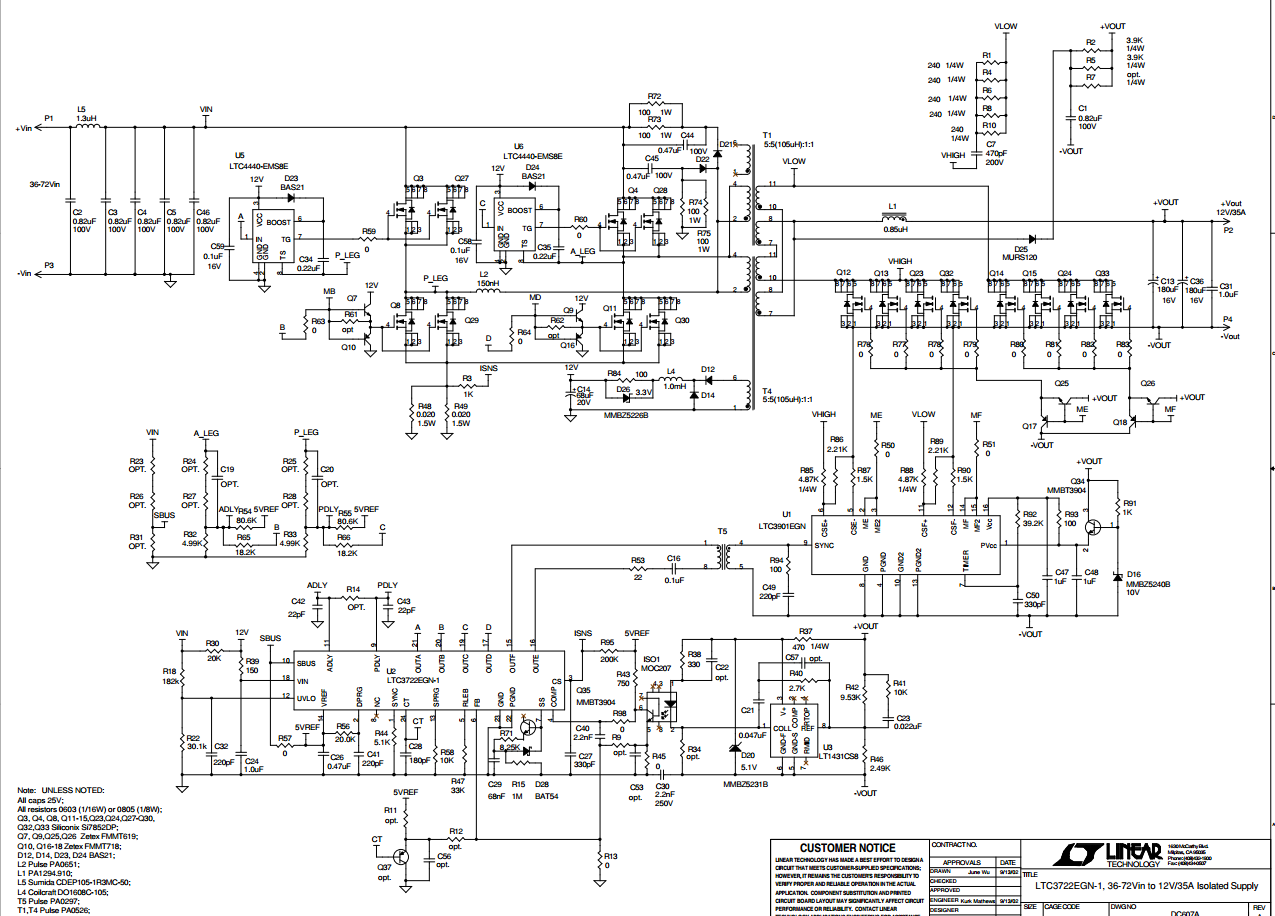
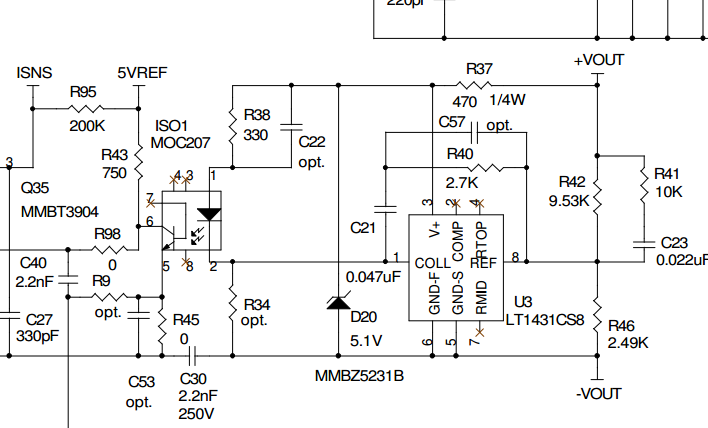
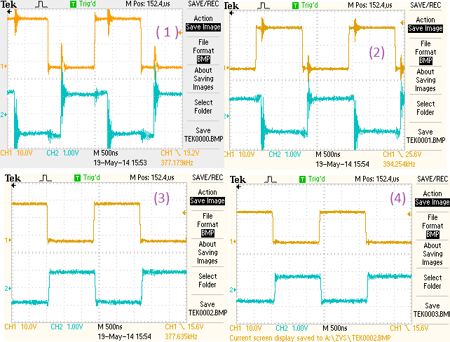
Currently i am  using a full bridge phase shifted converter with ZVS topology, i was given a design which had several faults within and have been working through them. Initially there as jittering on the high side MOSFET switching and noise from the magnetics which has been resolved. The design specification is a 24V DC to 350V DC, with a input range of 18V to 30V. Unfortunately when the input voltage drops below 24V the output also decreases. has anyone had similar issues in the past or have any idea what could be the issue, any help is much appreciated.

  • Hello,

    What controllers and Mosfet drivers are you using?

    Others may help you if you can attach the schematic and more details about the issue.

    Regards

  • The controller is a LTC3722-1 and the MOSFET drivers are LM5101ASD. The board is stable from 24.5V to 30V. When it reaches below 24.5V-23.8V noise is produced from the magnetics and the high side MOSFET switching becomes unstable. From 23.8V and below the output voltage seems to drop. I have changed the ZVS delay mode from adaptive to fixed. Also i have tweaked the feedback compensation loop with no effect on the issue. The board is designed with 120W power output at 350V. The oscillations frequency of the controller is 750kHz.It may be hard to upload the schematic due to my company policy on data security. However the design setup is similar to that of the controller development board, apart from the secondary side driver and the LM5101ASD drivers are used for both HI and LO MOSFET stages. Which can be seen attached. Is this a deep routed problem with a combination of component section, or a certain aspect of the design that has been done incorrectly?


  • Hello Liam,

    Your input range is quite large in most design the input range is 3:1.  When a phase shifted full bridge is used generally it is for a high input voltage range.  In most cases this device is used in telecom 36 to 72V range 2:1 or high power applications that require a PFC front end. When the PFC front end is fixed generally the full bridge is designed to operate with a 2:1 input range.

    There are a few reasons why your design may not be working.  Your transformer turns ratio is not designed for the low voltage input.  If you study the gates and current sense signal this will let you know why the design is not working.  You may also have issues with your feedback loop with such a wide input range.

    I am not sure what your end application is but the input range does not seem to be correct and will give you many issues.  If this an offline converter you probably should have a PFC boost front end to regulate the input voltage.  Also consider decreasing the input to less than 3:1 in your design.

    Regards,

  • The input range is from 18V to 30V doesn't this give a range of 1.66:1? The values that are illustrated in the demo board schematic in the picture vary in the design that I have been working on. The transformer turns ratio in the current design is np:4 ns:10, this being 3 transformers in parallel on the primary side and series on the secondary. This having a 330n inductor on the primary. I have looked at the current sense of the design and have changed it with a variable resistor to gauge the effect through the variable input voltage. Also i have looked at the high side ZVS overlap, when the input voltage is reduced the overlap reduces till the signals are completely out of phase,then the amplitude of the switching waveform reduces. The feedback has been complex in its nature from the research i have conducted , it has been a challenge getting my head around it to be honest. In what way will the variable input effect the feedback loop? Also what issue on the gates would result in a reduction of output voltage? Thanks for the reply any help is much appreciated as my lack of experience is apparent.

  • I misread the email.  I am not sure what benefit ZVS would bring with input voltage less than 30V.  I am not familiar with LT controller, maybe there is someone else on the forum that can help you with this unique design.

    Regards,

  • Ok, thank you for your support. Any help is appreciated. More information for anyone who can help.The feedback configuration in the designis as follows below


    The values for R40 and C57 have been changed for the application as this sets the feedback poles. The poles from the datasheet were calculated from the following formula.

    In the design Co=101.33uF, with a max load of 1K this give a minimum pole of 1.57Hz which didn't seem right to me. The zero pole has been calculated at 1254Hz and the maximum at 1576Hz with no load. Does this sound reasonable?

  • These are the high side switching waveforms of the MOSFET's with (1)=At 28V input with ZVS overlap (2)= 24V input (3)= Signal at cut off before the output reduces and (4) = At 20V with reduced amplitude.


  • Latest update, the power supply is regulated at the 350V output under 5k load, however when the 1k load is connected the voltage drops.

  • Problem solved under full load conditions the ZVS was reaching full duty cycle, with the minimum overlap achieved the voltage began to drop. Changing the transformer winding ratio allowed for the 350V to be achieved throughout the input voltages.