i'm trying to understand in more details how to design around the bq24401.
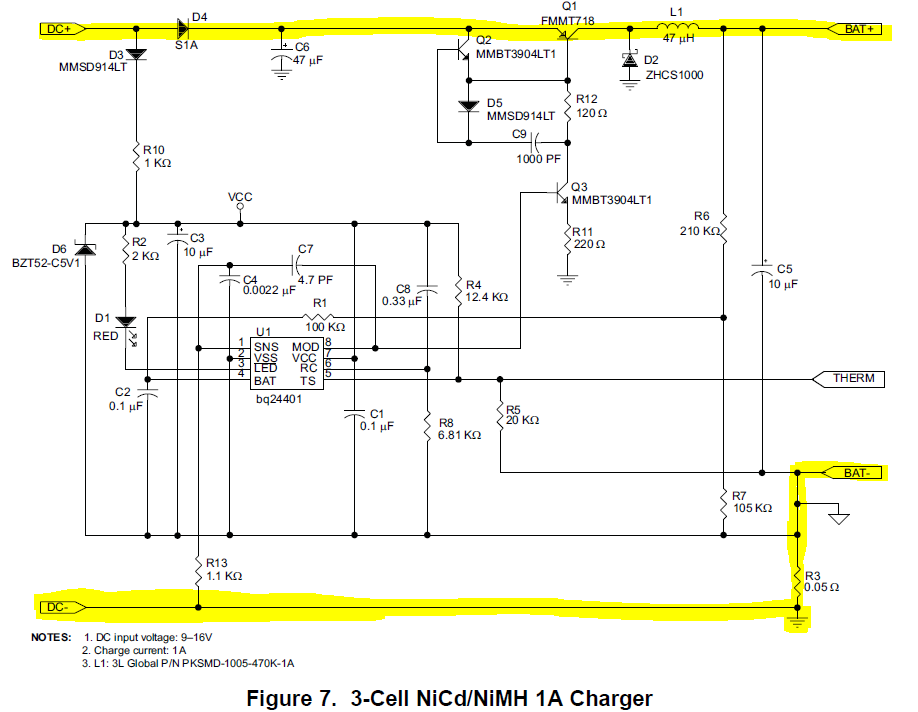
Can i please have an explanation of the current control circuit in figure 7, page 10 of the BQ24401 datasheet? 
thanks.
i'm trying to understand in more details how to design around the bq24401.
Can i please have an explanation of the current control circuit in figure 7, page 10 of the BQ24401 datasheet?
thanks.