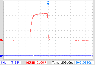
I have a new layout that is using the LM3488 to boost 11-17Vin to 25v/3A. Switching power supplies are new to me and I have been studying any information I can find over the past few weeks. I chose the LM3488 because it seemed simple and it was supported by Web Bench.
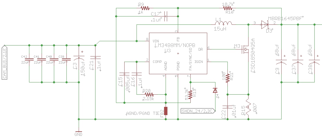
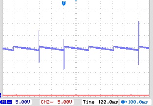
What I am seeing is an unstable output, but not sure were to look first. While unloaded, there are large ringing pulses at the switching fs. I can see significant ringing on the rising edge of the gate pulse. Over long periods, I can see a 200ms sawtooth waveform with periodic rings.
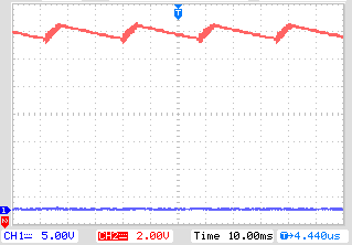
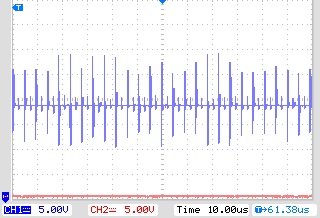
When I apply a small load (~400ma) the it looks to be stabilizing, but when I move to around ~800ma, the ringing is severe.
While the PCB layout is definitely not optimized, it seems the oscillation problem is more likely in the schematic. I will be sending in for a revision of the board on the next few days to fix issues with the main part of the circuit so I can clean up the layout as needed. For the moment though, I feel like I am missing something fundamental that prevents the circuit from being stable.
If anyone is inclined to point out where I should be looking first, I would be grateful.
Some basic grabs of the the scope....
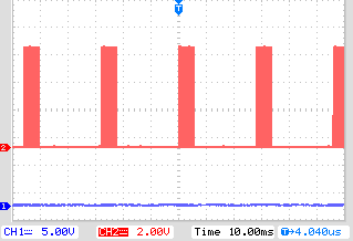
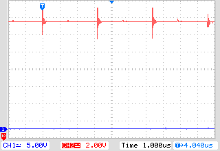
Gate pulse......
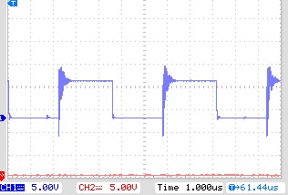
Output no load......
Output loaded....
Schematic with webbench values. I have studied the data sheet and calculated similar values. I have experimented with some parameters and saw no improvement. When I got to the point where I was just guessing, I thought I should ask for opinions.
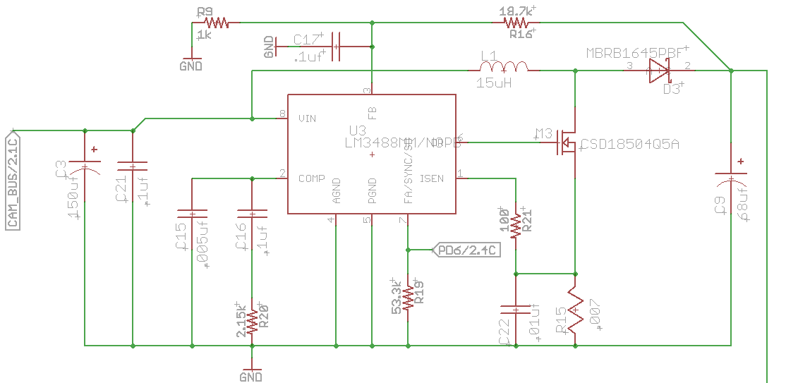
For the purpose of testing. My test PCB is only populated with the schematic above although the full circuit is much larger. There is also 3x 68uf caps in parallel on the output - the just the one shown in the schematic. ESR is around 8mOhms at 200uf. The PCB layout is hard to show because the power section is so close to the rest of the circuit - which may be confusing. If anyone thinks that this output can be fixed entirely in the layout - i will certainly figure out a way to show it.